MEMS Sensor Packaging Adhesive Selection: Die Attach to Cavity Sealing
SCITEO MEMS sensor packaging adhesive selection guide: grading rationale and failure mechanisms across low-stress, low-outgassing and wide-temperature interfaces
Abstract
Treating a micro-electromechanical system as a scaled-down digital IC is the most expensive lesson this device class teaches. Transistors inside a logic chip are static; packaging there means conduction, protection and heat removal. Inside a MEMS sensor the structures move: cantilevers, suspended proof masses, ultra-thin membranes, comb electrodes, micro-cavities. Every bit of residual stress, every cycle of thermally mismatched shear, every trace of contamination the package interface delivers to those structures lands directly in the output signal.
MEMS packaging is therefore closer to interface engineering. Mechanical stress has to be decoupled through stress isolation, the cavity has to stay clean and hermetic for years, and the finished device has to survive everything from cold storage to lead-free reflow peak. The difficulty is that these three demands pull against one another. Low modulus relieves stress but usually arrives with high expansion. Inorganic filler pushes CTE down and thermal conductivity up, and drives modulus up with it. Low outgassing demands a clean resin, while the line wants a generous flow and cure window.
What follows moves through demand structure, physical boundaries, SCITEO Advanced Materials' adhesive portfolio, device-level problems from the floor, and the production window, turning die attach, lid sealing, underfill, electrode protection, structural bonding and thermal interface classes into numbers that can be checked one item at a time.
Core Parameter Comparison
The table below places SCITEO MEMS interface systems alongside conventional industry practice. Grades are segmented by interface requirement and are not interchangeable:
| Parameter | SCITEO | Industry Norm | Test Standard |
|---|---|---|---|
| Applicable interfaces | Die attach, lid sealing, underfill, electrode protection, structural bonding | General die attach and full potting | Not applicable |
| Material temperature window | −55 to 300 °C (portfolio envelope to 500 °C) | −40 to 150 °C | TGA / long-term thermal aging |
| 260 °C reflow survival | Multiple passes, no popcorning or interfacial delamination | Elevated delamination and cracking risk | J-STD-020 |
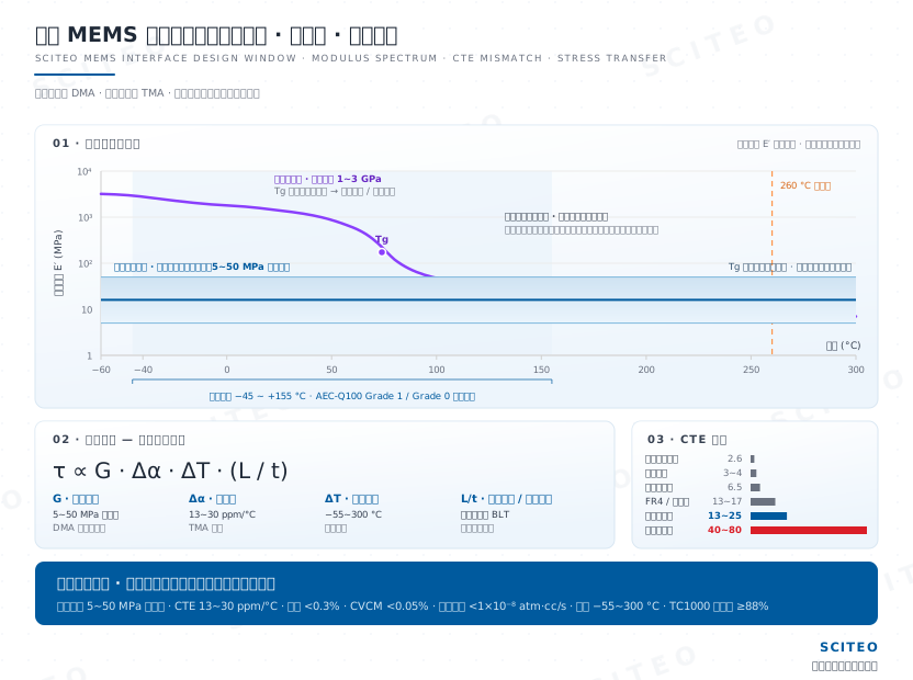
| Steady-state Young's modulus (tunable) | 5–50 MPa | 1–3 GPa | DMA |
| CTE (below Tg) | 13–30 ppm/°C | 40–80 ppm/°C | TMA |
| Cure linear shrinkage | <0.3% | 1–3% | ISO 2577 |
| Die shear strength | ≥18 MPa | 8–12 MPa | GB/T 7124 |
| Cavity leak rate (He, internal spec) | <1×10⁻⁸ atm·cc/s | 1×10⁻⁶ class | MIL-STD-883 Method 1014 |
| Outgassing (CVCM) | <0.05% | 0.5–1% | ASTM E595 |
| Volume resistivity (insulating / conductive) | >10¹⁵ / 5×10⁻⁵ Ω·cm | 10¹²–10¹⁴ Ω·cm | ASTM D257 |
| Thermal conductivity (tunable) | 2–20 W/m·K | 0.5–2 W/m·K | ASTM D5470 |
| Extractable ions (Na⁺/Cl⁻) | ≤10 ppm | 30–100 ppm | IC ion chromatography |
| Shear retention after 1000 thermal cycles | ≥88% | Visible decay | JESD22-A104 |
| Shear retention after 85/85, 1000 h | ≥85% | Visible decay | JESD22-A101 |
Demand Structure: MEMS Packaging Is Not a Shrunk IC Package
Mechanical Sensitivity Turns the Package into a Design Variable
A conventional digital package behaves, mechanically, like a rigid box: the die sits still, the solder balls carry electrical and mechanical load, and distortion inside the box matters only if it cracks an interconnect. MEMS sensors overturn that premise. A pressure sensor membrane is often only a few micrometers thick, an accelerometer proof mass hangs from a few micro-beams, a microphone membrane is thinner still, and a gyroscope drive mode resonates in the tens of kilohertz. What those structures share is that the quantity they measure is displacement.
The modulus, cure shrinkage, coefficient of thermal expansion and viscoelastic behavior of the adhesive layer are therefore no longer properties of assembly consumables. They are part of the metrology chain, and stress isolation moves from a structural-design requirement into a formulation one. Same wafer, same process flow, and a difference in die-attach modulus or bond-line thickness alone can shift the zero-output of an outgoing lot by a systematic offset. Once the mounting interface of a MEMS chip changes material, part of that device's as-built stress state has been redefined, which is why a material change on a MEMS line carries almost the validation weight of a process change.
A simple way to size the effect: interfacial shear stress scales with a shear-lag relation:
τ ∝ G · Δα · ΔT · (L / t) , G = E / [2(1 + ν)]
Here G is the adhesive's shear modulus, Δα the thermal mismatch, ΔT the temperature swing, L the transfer length from the die to its neutral point, and t the bond-line thickness. Softer adhesive, smaller mismatch and swing, shorter path, thicker bond line, and the interface delivers less stress into the sensing structure. The relation runs backwards just as well: take the allowable displacement at the most stress-sensitive structure, divide by the transfer path length to get the average strain the path can carry, then multiply by the effective modulus to back out the interface stress budget. Every link in that chain is measurable. Silicon's Young's modulus and Poisson ratio are known, substrate and adhesive CTE can be measured, the adhesive modulus spectrum comes from DMA, and what remains is interface geometry and cure shrinkage. Run that chain first and the selection usually collapses to one point: keep the adhesive's thermal expansion as close to silicon as possible. Drift is the signature failure metric on these devices and it comes down to CTE combined with cure shrinkage, so SCITEO keeps a settled family of low-CTE formulations, with die-attach grades selectable between 13 and 25 ppm/°C for head-to-head comparison.
Several Demand Curves Point at One Set of Interface Requirements
By Mordor Intelligence's latest estimate, the MEMS packaging market runs in the USD 8.51 billion class today and points to roughly USD 11.99 billion within five years, a 7.12% compound rate. What drives it has already turned over once: handset volume still underpins the base, but the delta now comes from edge intelligence — automotive safety functions that need low latency, on-device AI in phones that presses several sensors and compute dies into one footprint, and implantable monitors that have to satisfy hermeticity and sub-micron package tolerances at the same time. The structural figures matter more to a materials engineer: inertial devices hold close to 40% of revenue (39.78%), the largest single category; by platform, wafer-level chip-scale packages take 44.25% while system-in-package closes the gap at a 9.22% compound rate; and by material, organic substrates remain the workhorse while glass leads the growth tier at 10.3%, helped by maturing through-glass via (TGV) processes that add a vertical interconnect path on top of glass's hermeticity and CTE match, with RF MEMS and implantable devices pulling glass and ceramic demand along with it. Asia Pacific holds 47.3% of that revenue, where both capacity and adoption are concentrated.
Downstream, four curves run in parallel. Automotive is the leading driver, where safety-related functions route devices through the MEMS-specific AEC-Q103 qualification with temperature and cycling conditions set by grade. Consumer volume still rests on handsets, but the cleanliness and consistency demanded of acoustic and optical devices has risen sharply. Industrial automation pushes accelerometers, inclinometers and pressure transmitters toward long service life, wide temperature range and vibration exposure. Medical and implantable devices raise hermetic sealing and biocompatibility to admission criteria at the same time.
All four curves land on one set of intrinsic metrics: modulus has to be low and stay flat across the service window; shrinkage, CTE, outgassing and extractable ions all have to be low; and the cavity has to be hermetic. Those constraints have to hold simultaneously inside one formulation, and discounting them item by item does not work.
Three Hard Boundaries: Stress, Hermetic Cleanliness, Wide Temperature
Stress and Zero Drift
Thermal mismatch is the main stress source. Silicon runs near 2.6 ppm/°C, alumina ceramic near 6.5 ppm/°C, glass lids around 3 to 4 ppm/°C, FR4 organic boards 13 to 17 ppm/°C in plane, copper leadframes near 17 ppm/°C and aluminum structures above 20 ppm/°C. As the assembly cools from cure temperature or reflow peak to room temperature, those differences accumulate into interfacial shear stress and global warpage. If the adhesive stays rigid across the whole service window, that stress crosses the interface almost unattenuated and is delivered through the silicon into the sensing structure.
A second source is intrinsic: volumetric shrinkage as the resin crosslinks transfers straight into the die underside. Dropping shrinkage from 3% to below 0.3% buys as much as lowering CTE by a grade, and the two are achieved by completely different means, so the formulation has to treat them separately.
The third source is temporal. Every polymer is viscoelastic, responding with both elastic and viscous character: under cyclic load, strain lags stress, which reads out as loss tangent; under sustained load, chain segments slide, which reads out as creep. Low modulus only covers the transient case. What actually drives inertial bias stability (Bias Instability) is where the material's principal relaxation time sits: park it near the service vibration band and the residual bending moment from the substrate keeps driving irreversible micro-creep, so after a few months in the field the zero-rate offset (ZRO) drifts steadily in one direction.
Once the adhesive layer yields irreversibly, bond-line thickness drifts asymmetrically under the die and the flatness and coplanarity of the sensing structure go with it. For a piezoresistive pressure die, that is an asymmetric preload on the Wheatstone bridge. For a multi-axis inertial part, it is a twisted measurement reference.
The practical lever is a combination rather than a single metric pushed to its limit: hold cure shrinkage below 0.3%, put modulus in the band that neither transmits stress nor permits displacement, press the glass transition below the service floor and keep the storage modulus spectrum flat across the working range. SCITEO's low-stress die-attach system is qualified the same way: run the full 1000 cycles between −45 and 155 °C before quoting a figure, and shear strength still holds at 88% or better, rather than shipping initial strength.
Cavity Hermeticity, Cleanliness and Getters
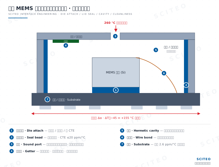
Many MEMS parts need a vacuum or inert cavity: infrared thermopiles and microbolometers, resonant pressure gauges, inertial devices, some microphones, RF MEMS and acoustic filters (SAW/BAW); for inertial and RF MEMS, wafer-level vacuum packaging has become standard process. A sealed cavity is a closed gas volume whose internal pressure tracks ambient temperature. Heat it and positive pressure pushes the interface outward; cool it and negative pressure draws external moisture inward. The breathing effect does not pick a convenient location, and the first point to give way is usually the corner with the smallest bond area and the highest stress concentration.
Hermeticity only means something when tied to a test method and a cavity volume. MIL-STD-883 Method 1014 converts fine-leak results into an equivalent standard leak rate in air and sets limits by internal free volume: a micro-cavity at or below 0.05 cm³ sits in the 5×10⁻⁸ atm·cc/s class, 0.05 to 0.4 cm³ relaxes to 1×10⁻⁷, and only above 0.4 cm³ does it become 1×10⁻⁶. The same method tightens a further decade for Class K space hybrids (1×10⁻⁹ / 5×10⁻⁹ / 1×10⁻⁸), which is the basis for pushing internal targets lower in high-reliability programs. Gross-leak screening uses fluorocarbon liquid under heat to look for continuous bubbles, or fluorocarbon pressurization with gravimetric verification. Equally important is internal water vapor, measured by residual gas analysis under Method 1018 and commonly specified at 5000 ppm. That figure decides whether the cavity condenses on its internal surfaces over a long thermal-cycling life.
Vacuum cavities also carry a getter. Thin-film getters need activation before use, and conventional non-evaporable getters (NEG) want 300 to 400 °C, which means every organic material inside the cavity has to survive that step and hold on to the moisture and hydrocarbons it has already adsorbed. Otherwise the getter is poisoned by the very materials meant to protect it. That physics splits practice into two routes: switch to a getter that activates at 150 to 250 °C, or activate and pump down first, then use localized laser or infrared heating to put the heat only on the seal region so the adhesive never crosses its decomposition threshold. Below 10⁻³ mbar, most ultra-high-vacuum parts skip organic adhesive altogether and go to eutectic or metal bonding. SCITEO supplies a low-outgassing seal grade for this cavity class, with collected volatile condensable material (CVCM) held below 0.05% and a 300 °C tightened retest available for customer verification.
Cleanliness is a parallel line. Wafer-level bonding and lid attach usually run at Class 10 or better, because a single micrometer-scale particle on the bond interface props open a void that breaks local hermeticity and distorts the optical surface at the same time. Cleanliness also has a chemical dimension: contamination of a microphone back volume, an optical window or a micro-mirror surface is usually a chemical event first, and only surfaces as degraded device metrics days to weeks later; and a movable structure bridged by residue can stick outright (stiction).
Wide Temperature, Damp Heat and Reflow
The temperature boundary has at least three segments. At the cold end, automotive parts are qualified by grade, with Grade 1 spanning −40 to +125 °C and Grade 0 reaching +150 °C; industrial and outdoor applications also consider lower storage temperatures. At the hot end, devices have to operate long-term near 125 to 150 °C, and higher in some engine-bay and downhole duties. In between sits a process temperature: modules must survive 260 °C peak lead-free reflow and carry the matching moisture sensitivity level (MSL), and some acoustic devices specify a 260 °C, 50-second reflow tolerance outright. SCITEO's high-temperature range leaves margin on that step, and its delivery figures quote shear retention and void-free C-SAM imaging after three consecutive 260 °C lead-free passes, not a bare peak-temperature rating.
Those three segments do not ask the same thing of the material. The cold segment tests the flatness of the modulus spectrum and low-temperature toughness; if the glass transition falls inside the service window, the adhesive hardens on the cold side and softens on the hot side, losing on both. The hot segment tests thermal and oxidative stability of the crosslinked network, which calls for a TGA decomposition onset plus long-term isothermal aging data. The reflow segment tests low-stress behavior under a transient thermal shock and low moisture absorption, because absorbed water vaporizes at peak temperature, and the more vapor there is, the higher the risk of popcorn cracking.
Damp heat is what happens when those boundaries stack. Steady-state bias at 85 °C/85% RH, pressure-accelerated HAST at 130 °C/85% RH, and high-temperature storage form a sequence in which the real risk sits in the order, not in any single step: reflow creates residual stress and micro-cracks first, damp heat then plasticizes the adhesive and pulls modulus and Tg down together, and thermal cycling drives the accumulated damage to the interface. SCITEO reports 90% or better retention after 1000 h of high-temperature storage at the 200 °C grade and 85% or better after 1000 h of 85/85, both run on the same set of samples in series rather than scored as isolated tests.
The two automotive temperature grades are not the ceiling. Temperature sensing, PTC heating and thermal-management modules run long-term in engine bays, photovoltaic storage and smart-grid equipment, while petrochemical, gas-turbine and aero-engine flow paths push pressure devices into 300 °C and even 400 °C of continuous duty. Silicon-to-glass anodic bonding and glass frit are what usually hold the cavity hermetic in that class, and silicon carbide piezoresistive devices already reach the 600 °C order. What this duty asks of an adhesive lands on strength and insulation retention after long-term aging; a transient peak rating says nothing. SCITEO matches it with several long-term high-temperature grades at 200 °C, 300 °C and 400 °C, picked against actual service temperature and duration rather than a transient peak. Picking a grade means naming three quantities together: service temperature, sustained duration and thermal-cycle count. Leave any one of them out and the selection drifts.
The Engineering Range of MEMS Adhesives
SCITEO answers the MEMS adhesive question with a range graded by interface position, covering six of them: die attach, lid and cavity sealing, underfill, electrode protection, high-temperature bonding and thermal interface. Insulating, conductive, thermally conductive, wide-temperature and low-stress grades all coexist, so the different interfaces on one device can be specified separately instead of forcing a single adhesive to cover everything. The reason is straightforward: adhesive demand is not concentrated at one point on a MEMS part. Unfolded by process step, each position has its own failure modes and material metrics, and one formulation that tries to cover all of them usually fails at one.
Die Attach: Low-Stress Grades Versus Conductive Silver
A MEMS chip's die attach is the most sensitive step in the whole flow. It has to hold position, decouple stress, match the expansion of the substrate, and remain compatible with the dispense or placement process. The insulating low-stress grade covers the vast majority of sensor dies, with the goal of low modulus and low shrinkage so that elastic deformation replaces rigid transfer. The conductive silver grade handles positions that need electrical grounding, such as electrostatic discharge, shielding and return paths, and dies that require a substrate potential. Volume resistivity there is usually specified in the 10⁻⁴ to 10⁻⁵ Ω·cm class, with thermal conductivity above 5 W/m·K alongside it.
Neither route can be picked off a label alone. The conductive network of silver flakes raises modulus sharply: the higher the loading and the better the conductivity, the stiffer the adhesive and the less stress it decouples. For pressure and inertial devices the working point is usually a compromise between conductivity and low stress, not the lowest resistivity on the datasheet. Another easily overlooked property is position retention: micrometer placement tolerances require the adhesive not to spring back or slide once placement pressure is released, which is a rheology problem defined by yield stress and thixotropic recovery rate. SCITEO's die-attach grades specify both dimensions together, holding the conductive grade at 5×10⁻⁵ Ω·cm while keeping modulus inside a tunable band. When grounding need and stress ceiling pull against each other, that is a formulation problem to settle up front, not something to discover after placement.
Lid and Cavity Sealing: Three Routes Coexist
Lid and package sealing runs three mainstream routes, and the route chosen decides what role the adhesive plays.
A glass lid bonded directly to the die (glass-on-die), or fixed to the package body to close a cavity (glass-on-housing), is common in optical devices and some infrared devices. Failure concentrates in three places: cavity pressure loading as temperature changes, interfacial residual stress from cure shrinkage, and local hermetic defects caused by particles or voids. Mature practice splits the sequence into two steps: B-stage pre-fixation gives the lid handling strength right after pick-and-place so final cure cannot shift or bleed it, while the bead stands in a narrow, tall cross-section, which is what turns bond-line thickness and seal width into controlled quantities. The fourth failure mode is not one of those three: glass surfaces are rich in silanol groups (Si-OH) that water attacks readily at 85/85, so once the interface hydrolyzes it debonds in one piece, and glass's low CTE concentrates the interfacial shear further. The more glass in the design, the more the hydrolysis-resistant coupling network matters.
Metal or ceramic packages switch to solder or eutectic sealing. Au-Si eutectic and Au-Sn solder bond far above any organic adhesive and give a structural hermetic barrier, at the cost of harder cooling stress that only CTE matching and structural design can absorb — not something an adhesive can take on.
Glass frit sits between the two, forming a hermetic joint from an inorganic sealing material with good temperature capability, at the cost of a high sealing temperature and a demanding requirement on how complete the front-end device is. An organic sealant here is rarely a replacement; it is backfill: pre-fixation, local strain relief, and semi-hermetic sealing where a full hermetic class is not required. SCITEO supplies both insulating and conductive lid-seal grades at this stage; the insulating grade holds CTE within 20 ppm/°C, the conductive grade pairs EMI shielding with hermeticity, and both are re-verified for strength and leak rate after 260 °C reflow and 85/85 aging.
Underfill and Dam-and-Fill
Flip-chip and bump-based packages raise interconnect density, and the price is that nearly all interfacial shear lands on the bumps. Underfill has to complete a gap of a few tens of micrometers by capillary action and spread the CTE mismatch stress across the whole die footprint. Published work consistently reports that a complete fill raises flip-chip solder-joint thermal fatigue life by one to two orders of magnitude, while an incomplete fill, trapped voids, or a poorly chosen Tg gives that gain straight back.
Underfill on MEMS parts carries two more constraints. The gap is narrower, so filler particle size has to match the minimum gap; a large particle bridging a narrow passage blocks the flow path outright, and the working rule is that maximum filler size should stay below one-third of the smallest gap. The device is also more stress-averse, so the underfill Tg has to sit above the service ceiling rather than inside the range; otherwise the layer softens and stiffens repeatedly around Tg during a −40 to 125 °C cycle and concentrates stress back onto the bumps. Dam and fill is used where the flow boundary must be controlled, with the dam holding the line and the fill handling sealing and buffering.
SCITEO's low-stress underfill grade puts Tg above 150 °C and CTE in the 13 ppm/°C class, with filler particle distribution matched to each customer's minimum gap.
Electrode Protection, High-Temperature Bonding and Acoustic Dams
Electrodes and bond areas need moisture, corrosion and vibration protection without being locked rigid. A low-modulus gel or a flexible silicone suits this better than a rigid epoxy: it forms a protective layer while leaving displacement room for the die and the wire bonds, and fixation that must sit at sustained high temperature goes to the 200 °C-and-above grades. For pressure devices exposed to oil and fuel vapor, a fluorosilicone adds one more barrier against media permeation. These protection materials are usually picked as low modulus plus low moisture absorption, so the layer does not become a stress source or a moisture path itself.
The dam and housing seal on an acoustic device is a separate class. The seal line on the package is often compressed to the 150 to 200 micrometer range and sits immediately next to an under-port sound hole. The bead has to cut off cleanly under high-speed jetting and then build an anti-slump structure the moment it lands, otherwise a tail lands over the membrane or a slump creeps into the sound port. The governing parameters are thixotropic index and post-shear viscosity recovery time, followed by the uniformity of the cure temperature profile; a degree-of-cure gradient across one part will cost the lot its frequency-response consistency.
High-Thermal-Conductivity Interfaces
Power devices, micro-mirrors, infrared detectors, ultrasonic transducer arrays (PMUT/CMUT), inkjet printheads, and modules that co-package readout circuits with power management demand low stress and thermal conduction at the same time. Thermally conductive filler is where stiffness comes from: spherical alumina delivers 2 to 5 W/m·K while keeping modulus relatively low, and the next conductivity tier up leans on aluminum nitride and similar ceramic fillers, with modulus rising right along with it. Grading by heat-flow path is the safer route: use a low-modulus, medium-conductivity grade from die to substrate to preserve stress decoupling, and a high-conductivity grade from substrate to heat sink for lateral spreading, keeping its stress influence away from the die.
The metric to watch on acceptance is interfacial thermal resistance; bulk conductivity does not describe the whole heat path. A 25 micrometer bond line carrying 5% void area typically raises effective thermal resistance more than moving up one conductivity grade would recover, so conductivity grades have to be accepted together with void rate and bond-line thickness. SCITEO delivers thermal grades across 2 to 20 W/m·K segmented by heat-flow path. Where the die-to-substrate and substrate-to-heat-sink segments sit on two different grades, the two interfacial resistances are quoted separately, each with its measured value at the specified bond-line thickness.
Device-Level Process Problems
The same evaluation basis ranks differently from one device to the next. What the floor actually raises is rarely a material parameter; it is a concrete symptom, such as a lot drifting out of zero tolerance after installation, microphone sensitivity scattering across a batch, or pins greening after salt spray. Translating those symptoms back into material variables is where selection starts. The five device classes below cover the problems that come up most often, and the formulation variables SCITEO typically moves for each.
Pressure Sensors: Oil-Filled Cores, Media Compatibility and Thermal Drift
The core of a MEMS pressure sensor is a silicon membrane etched thin, carrying four piezoresistors in a Wheatstone bridge. The thinner the membrane, the higher the sensitivity and the more sensitive the part to interface stress. Two structures dominate in practice: direct-contact and isolated-diaphragm.
In the direct-contact type, the measured medium reaches the die through a port, and the adhesive layer and die backside are exposed to it. This structure is the most demanding on materials: oil, condensate and acidic exhaust all start working on the adhesive and the interface. A fluorosilicone system earns its place here through low surface energy and a dense structure, resisting oil permeation while blocking moisture. SCITEO treats fluorinated chain density as a tunable variable on this grade and re-tests immersion and permeation against each customer's media list instead of offering one generic part number.
The isolated-diaphragm type seals the die inside a 316L stainless steel base and transfers external pressure through silicone oil, so the die never contacts the medium. Sealing on this oil-filled core is done by laser welding, and the adhesive's job becomes internal fixation and stress buffering. The critical conflicts then shift to two: oil compatibility, since a layer that swells or leaches under long immersion changes the transfer characteristic; and the thermal expansion difference between oil and adhesive, which adds internal pressure during thermal cycling. Both are solved by material selection, not by process compensation.
Zero drift and hysteresis are the long-running theme. Zero temperature coefficient, full-scale temperature coefficient, nonlinearity and hysteresis together define usable accuracy, and the common application set covers automotive intake-manifold pressure, tire-pressure monitoring (TPMS), and ventilator or oxygen-concentrator pressure sensing. Algorithmic compensation removes part of the repeatable error but cannot remove irreversible drift caused by phase transition and creep in the adhesive layer. That is why many pressure-sensor compensation models converge in the lab and then drift out of spec in the field as thermal cycles accumulate.
Inertial Devices: Quality Factor, Quadrature Error and Bond-Line Thickness
A high-performance MEMS gyroscope works through micro-amplitude, high-frequency oscillation of a proof mass at a specific resonance, sensing a weak capacitance change on an orthogonal detection axis through the Coriolis force. Its core metrics are mechanical quality factor (Q) and bias stability.
Q is more sensitive to the package environment than it usually gets credit for. Residual gas molecules in the cavity create squeeze-film damping that carries resonant energy away, and once Q drops, the drive circuit can only raise drive voltage and amplify the noise floor. That is why inertial devices demand vacuum packaging, and why the getter exists. Micro-voids at the die-attach interface, non-uniform thickness, or intrinsic material damping act as escape paths for acoustic energy from the silicon into the substrate and pull Q down the same way.
Quadrature error comes from lost symmetry in structural stiffness. Anisotropic residual strain left by cure and cooldown decouples the natural frequencies of the drive and sense beams in an uncontrolled way, which appears at the output as a large spurious signal unrelated to angular rate and eats directly into the detection circuit's dynamic range. The countermeasures split in two: on the material side, minimize loss tangent and the anisotropy of cure stress; on the process side, tighten bond-line thickness tolerance so the mechanical boundary under the die stays symmetric.
Thinner is not automatically better here. Too thin cannot buffer, too thick adds thermal resistance and instability, and thickness consistency matters most of all. SCITEO suspends a batch of microspheres with a highly uniform diameter in the formulation; under placement pressure they act as micro-stops that physically lock bond-line thickness, which measurably lifts resonance-frequency consistency across the lot.
Acoustic MEMS Microphones: Narrow Beads, Sound Ports and Reflow
Acoustic MEMS microphones — silicon mics, in industry shorthand — ship in the largest volume, at the lowest unit value, with the least tolerance for error. A typical package holds an acoustic sensing die, a dedicated readout ASIC, a metal lid with an acoustic port and an organic composite substrate, all within millimeter dimensions and under 0.04 grams, with a sound port only a fraction of a millimeter across.
The first gate is reflow. Many device datasheets specify a reflow window of roughly 50 seconds at 260 °C to suit surface-mount lines. Reflow peak causes two problems at once. Assembly stress stored in the adhesive and substrate releases instantly and warps the ultra-thin membrane, changing the micro-capacitance gap, distorting high-frequency response and dropping signal-to-noise ratio. At the same time, absorbed moisture vaporizes at peak temperature and, if a delamination front already exists, expands along the interface.
The second gate is acoustic sealing with a clear sound port. The seal has to be airtight: foam that only seals under heavy compression is not a reliable answer, whereas a rubber or silicone material that is inherently impermeable is. Bottom-port parts complete the board seal by soldering; top-port parts have to seal with a gasket on a limited top surface, which is harder. Any leakage shows up as lot-to-lot spread in sensitivity and frequency response, plus an added path for environmental noise.
The third gate is dispensing. The narrow bead has to stand, cut cleanly and not creep, and neither the sound port nor the back volume can be contaminated. Thixotropic recovery rate is the key parameter, and so is staged curing: anchor the geometry at a lower temperature first so the polymer has free volume to relax polymerization shrinkage during network formation, then complete the cure, so the membrane comes out of the oven near a low-stress neutral state; the cure profile therefore has to be re-calibrated to the oven rhythm, and the degree of cure in shadow zones assessed separately.
There is also an often-ignored constraint list. Cleaning, ultrasonic exposure, air blow-off and nozzle handling all have boundary conditions on a finished device; the sound port is sensitive to water and airflow, so material selection has to account for surface tension and moisture absorption to keep secondary line operations from turning good parts into scrap.
Optical MEMS and Micro-Mirrors: Cleanliness, Heat and Cure Shift
Micro-mirrors, optical switches and two-dimensional scanning devices for optical communication deflect continuously at kilohertz rates to steer and fold a beam precisely; single-photon avalanche diode arrays and indirect time-of-flight (iToF) modules on the LiDAR receive side live under the same cleanliness and heat constraints. Their interface requirements land on cleanliness, heat transfer and cure shift, and the weighting differs by device.
Any condensate inside a sealed optical cavity preferentially deposits on the cooler or laser-illuminated surfaces, becoming a scattering center that reduces mirror reflectivity over long operation and distorts the spot. Outgassing control for organic materials inside the cavity is therefore set at an optical grade, with collected volatile condensable material typically held below 0.05%, and tighter in some programs.
Rising temperature in the mirror support frame is the second line. High-power near-infrared pulses or compact drive electronics create meaningful heat flux, and that temperature rise changes the stiffness of the torsion beams, shifting resonance and degrading scan-angle accuracy. Low modulus and high conductivity are still in tension within one formulation, so grading is still how it gets solved: keep the micro-mirror mounting interface at low modulus to avoid distortion, and disperse surface-modified thermally conductive filler through the system to carry heat from the mirror body to a ceramic heat sink.
For optical devices that rely on active alignment or precision assembly, cure-stage volume change is the constraint. Any volumetric change during cure hands the alignment accuracy straight back. Dual-cure systems have a clear advantage: ultraviolet or visible pre-fixation gives the layer handling strength within seconds, and the subsequent mid-temperature cure crosslinks in a constrained state with far less shift than a purely thermal cure. Illumination geometry matters just as much, since symmetric placement of sources around the circumference avoids the asymmetric shrinkage that a one-sided first cure produces. SCITEO holds cure linear shrinkage below 0.6% on this optical dual-cure grade and builds shadow-zone supplemental heating around each customer's source layout.
Medical and Microfluidic Devices: Sterilization and Low Ionic Leaching
Continuous glucose monitoring (CGM) probes, lab-on-a-chip systems and implantable neural electrode arrays operate in whole blood, interstitial fluid or high-salinity electrolyte. These devices place a two-way requirement on packaging materials.
On one side, the material must not release active species into the fluid. Free amine curing agents, heavy-metal organotin catalysts and low-molecular oligomers that leach out can interfere with enzyme activity, break the electrochemical balance at a microelectrode, or provoke tissue response. Formulations therefore take a high-purity purification route, avoid aromatic amines and heavy-metal complexes, and build every diluent component into the main network so no migratable residue remains.
Process endurance is the other line. Microfluidic chips typically see periodic aggressive polar cleaning, and on the way out of the factory they pass 121 °C saturated steam, ethylene oxide or radiation sterilization. High temperature, pressure and oxidizing chemistry attack the bond interface and the channel seal together, and once a micro-leak or interlayer disbonding appears, the whole channel is lost. The formulation lever is a hydrolysis-resistant backbone with multi-scale coupling groups so the layer forms a dense interlocking interface against polycarbonate, cyclo-olefin copolymer, glass and silicon. SCITEO holds extractable ions within 10 ppm on this class and lists seal integrity after repeated sterilization as a release item.
The Production Window: Rheology, Dispensing and Cure Kinetics
Even excellent molecular design has no value if it cannot be turned into yield on a customer's high-speed line. MEMS packaging materials are bound to dispensing fluid dynamics, placement tolerance and the cure oven profile, and the questions from the floor cluster around a few symptoms: stringing at the needle, a blocked sound port, voids under the die, or a whole batch reading off-zero. Three points are the common source, and all three are variables SCITEO aligns during formulation.
Void-Free Filling
A bubble a few tens of micrometers across inside a bond line is a discontinuity in both mechanical stiffness and thermal resistance. In the next thermal cycle it becomes a stress concentrator that tips the die, and under vibration testing it readily grows into a through-crack.
Micro-voids come from three sources: gas entrained at the needle during high-speed dispensing, air trapped where the adhesive fails to fully wet micro-grooves on the substrate, and vaporization of volatiles during ramp-up. The matching material levers are three. Control de-aeration and filling so fewer micro-bubbles ship in the syringe. Match surface tension to lower the dynamic contact angle, so the flowing front pushes air out of the micro-grooves as the die is pressed down. And shape the onset of the cure reaction so it is gradual, leaving a path for gas to escape. SCITEO folds these three levers into two deliverable release metrics — as-shipped microbubble level and dynamic contact angle — rather than waiting for a customer to scan voids on the line and then reopen the formulation.
Acceptance relies on non-destructive inspection. Acoustic microscopy (C-SAM) scans the die-attach layer and lid interface with void area fraction as the release metric; highly conductive grades are also checked by X-ray for the solder or silver layer. Void limits vary widely by application, and IPC-7095E splits them into classes for ball grid arrays, where voids at the attach interface are more damaging than voids inside the ball. Acceptance thresholds typically tighten from 10% to 2%, with automotive and power grades the strictest.
Bleed-Out and Bond-Line Thickness Control
Resin bleed-out is the most common source of lot scrap in MEMS packaging. If the resin molecular weight distribution is too broad, low-molecular-weight fractions in a low-viscosity adhesive migrate along substrate traces under capillary force during ramp-up, contaminating wire-bond pads into non-stick opens or creeping into a motion cavity to seize a suspended structure.
Control has two halves. On the formulation side, narrow the resin's molecular-weight distribution to strip out free low-molecular fractions, then build in a temperature-triggered micro-network so the adhesive neither slumps nor bleeds through the early ramp but instead gels into a physical anchor as temperature rises, locking the macroscopic geometry. On the process side, pair the dispense pattern with placement pressure to hold bleed distance within a few tens of micrometers of the die projection edge.
Bond-line thickness control runs in parallel. For high-frequency resonant devices and inertial parts that need axial isolation, lot-to-lot bond-line thickness spread maps directly onto resonance-frequency consistency and cross-axis coupling. The microsphere stop described earlier is the passive answer; the active answer is to tune the rheological damping so the adhesive does not push back when placement pressure is released, which removes die tilt.
Low-Temperature Cure, Dual Cure and Stress Relaxation
Many MEMS dies already integrate precision readout circuitry on the front end, or use temperature-sensitive organic optical layers and flexible substrates that cannot take a long high-temperature bake. A latent cure system opens a window here: full crosslinking at 80 to 100 °C minimizes the thermal shrinkage differential during cooldown, while a one-part adhesive still gives several days of working life on a room-temperature line. SCITEO's latent low-temperature grades write both the final degree of cure in that window and the room-temperature working life into the delivery spec.
Ultraviolet and thermal dual cure suits processes that must lock position the instant the die is placed. After placement, a brief exposure at a specific wavelength forms a rigid locating frame at the bead edge and locks the spatial coordinate; the part then enters a conventional oven where mid-temperature heat activates deep crosslinking in shadowed regions. This route unifies takt time with strain dissipation, but the cure state in shadow zones has to be evaluated separately, otherwise an undercured region shows up later as strength scatter or anomalous outgassing.
Cure profiles should be designed against measurable evidence: DSC gives the reaction exotherm peak and residual enthalpy to confirm the cure is complete, and TMA and DMA verify that cured CTE and modulus spectrum hit design targets. The value of a stepped ramp is that internal stress is released in stages inside the oven rather than being locked into the interface by a rapid cure. The ramp is derived from the customer's oven and takt, with degree of cure treated as a batch release item. Degree of cure is not submitted apart from shear strength; the two only mean something read as a pair.
Selection Reference Table
The table below compresses the mechanisms above into criteria a packaging or process engineer can check line by line in review. Work it in order: lock the failure mode and primary metrics by interface, submit strength, insulation, outgassing and leak rate in pairs, then run the whole thing as a reflow, damp-heat and thermal-cycle sequence. Material metrics rarely stand alone: reading Tg without CTE, or leak rate without cavity moisture, leaves a conclusion that will not hold. What the customer actually rules on is still the before-and-after zero, sensitivity and signal-to-noise data around encapsulation.
| Interface | Typical Failure Mode | Primary Metrics | SCITEO Direction |
|---|---|---|---|
| Sensor die attach | Thermal mismatch stress driving zero drift and hysteresis | Steady-state modulus 5–50 MPa, CTE 13–30 ppm/°C, shrinkage <0.3% | Low-stress die-attach grade (tunable modulus) |
| Die attach requiring electrical ground | High grounding impedance, weak ESD discharge path | Volume resistivity 10⁻⁴–10⁻⁵ Ω·cm with low modulus retained | Low-temperature-cure conductive silver grade |
| Lid and package sealing | Cavity breathing driving leak-rate nonconformance, internal condensation | Internal spec leak rate <1×10⁻⁸ atm·cc/s, CVCM <0.05% | Hermetic seal grade (low outgassing, insulating and conductive) |
| Flip-chip and bump underfill | Voids, delamination, bump fatigue fracture | Tg above service ceiling, CTE match, capillary flow | Low-stress underfill grade |
| Electrode and wire-bond protection | Moisture corrosion, vibration fatigue | Low modulus, low water absorption, insulation | Flexible gel and protection grade |
| Acoustic dam and housing | Stringing, bead creep into the sound port, response scatter | Thixotropic index and recovery rate, staged low-temperature cure | Acoustic packaging grade (narrow bead) |
| Optical devices and micro-mirrors | Cavity condensation, resonance-frequency drift | CVCM <0.05%, 2–20 W/m·K, small cure shift | Optical-cleanliness and high-conductivity grades |
| Power and infrared devices | High interfacial thermal resistance, local hot spots | Low void rate, controlled interfacial resistance, low stress | High-conductivity interface grade |
Conclusion
Half of a micro-electromechanical system's performance ceiling sits in the die design and half at the packaging interface. The micro-structures determine how small a displacement the part can sense, and the interface's stress, hermeticity and cleanliness determine whether that sensitivity holds to the end of service life. Neither substitutes for the other, and both have to be right at once.
SCITEO Advanced Materials works on this interface as a formulation R&D partner rather than a catalog supplier, which is why the engagement starts upstream of the customer's structure and duty cycle. Read the real margin on the stress, thermal and cleanliness boundaries first, then decide which direction modulus, CTE, thermal conductivity, electrical conductivity and cure kinetics each need to move. Pressure, inertial, acoustic, optical and biomedical devices each have a matching delivery grade on SCITEO's formulation platform, and the different interfaces on one device can be specified independently and aligned on site to the customer's dispenser and cure takt. The further a device moves into extreme duty, the more it needs that kind of molecule-level collaboration, which is where SCITEO has kept its investment in semiconductor packaging.
This article is SCITEO Advanced Materials original technical content; unauthorized reproduction is prohibited.
Appendix: Process & Engineering Adhesive FAQ Index
Is a lower modulus always better for MEMS die attach? How is the window actually set?
No. Modulus decides two things: whether the stress peak is spread out, and whether the layer can hold the die in place under vibration and shock. Pressure sensors and accelerometers care about the first, so the adhesive should stay rubbery across the service window and absorb strain. High-frequency resonant parts and modules that must pass drop testing care about the second, and a modulus that is too low brings displacement and damping problems. The steadier route is to work from the allowable strain at the most sensitive structure, back out a modulus band, then check that the band stays flat across the whole temperature range rather than reading a single room-temperature point. SCITEO tunes this grade continuously between 5 MPa and 50 MPa and ships the DMA spectrum with the sample, so flatness across the service window can be checked point by point.
What basis should be used to accept the leak rate of a cavity sealant?
Never a bare number. It has to be tied to a method and a cavity free volume. MIL-STD-883 Method 1014 converts fine-leak results into an equivalent standard leak rate in air and sets limits by internal free volume: a micro-cavity at or below 0.05 cm³ sits in the 5×10⁻⁸ atm·cc/s class, 0.05 to 0.4 cm³ relaxes to 1×10⁻⁷, and only above 0.4 cm³ does it become 1×10⁻⁶. Review should confirm that the volume used in the conversion matches the actual package, that helium pressurization and dwell follow the method, and whether the reported figure is measured or converted. SCITEO's internal target on micro-cavity sealing grades reaches the 1×10⁻⁸ atm·cc/s class.
MEMS microphone lid dispensing keeps stringing or creeping into the sound port. What fixes it on the material side?
The root cause is rheology, not strength. Stringing comes from over-entangled chains and long relaxation times, so the fluid cannot break off by capillary pinch-off within milliseconds when the jet retracts. Creep comes from insufficient low-shear yield stress, so a droplet wets too far under surface tension after impact. The direction that works is faster thixotropic response: strong shear thinning under the valve for a clean cut, and recovery of structural viscosity within milliseconds once shear returns to zero, pinning the bead to its geometric boundary. A narrow, tall bead cross-section at 1.5 to 2.5 aspect ratio combined with thixotropy is what holds bleed within a few tens of micrometers of the die edge and keeps the under-port sound hole and back volume clean.
Why does an automotive part pass at room temperature and then fail thermal drift hysteresis in cycling?
Passing at room temperature shows the cure is complete, not that the modulus behaves across temperature. Conventional modified adhesives with uneven crosslink density, or with broad-boiling plasticizers, undergo secondary transitions near −30 to −40 °C, where modulus rises sharply and thermal contraction stress can no longer be absorbed by the layer, so it projects straight into the silicon membrane. On the hot side, the frozen segments then slide irreversibly and the stress relaxes. After one round trip the bond-line geometry no longer returns, so strain traces a hysteresis loop that no compensation model can converge on. SCITEO pushes the glass transition below the service floor, keeps a flat rubbery plateau across the working range, and suppresses segment sliding with a uniform crosslinked network.
A device has to survive 260 °C lead-free reflow. How does a low-modulus adhesive take that heat?
Low modulus and high-temperature endurance do not come from the same mechanism, so the design has to be layered. A flexible backbone provides low modulus and strain absorption; a rigid heterocyclic or high-bond-energy skeleton keeps the layer from softening or degrading at reflow peak; and interpenetrating networks or block structures lock the two together. The Si-O backbone carries notably higher bond energy than a C-C single bond, with free segment rotation, which suits a flexible matrix, while aromatic-heterocycle high-temperature resins carry the cohesive strength at peak. Acceptance should not stop at initial shear strength: it should look at retention after reflow and after aging, plus delamination by C-SAM.
For microfluidic and biomedical devices, how do ionic leaching and sterilization balance?
They pull against each other. Sterilization by 121 °C saturated steam, ethylene oxide or radiation requires the layer to resist hydrolysis and disbonding; and the biological interface is highly sensitive to leachables, because free amine curing agents, organotin catalysts and oligomers entering the fluid can disturb enzyme activity or the electrochemical balance at an electrode. SCITEO therefore takes a high-purity purification route, avoids aromatic amines and heavy-metal complexes, and uses a hydrolysis-resistant backbone. On acceptance, put extractable ions (Na⁺/Cl⁻) at or below 10 ppm, CVCM, and post-sterilization shear retention on the same release sheet. Passing one of them does not release the grade.