PROCESS // END-TO-END PACKAGING
Semiconductor Packaging
Resolving fine-pitch stress in heterogeneous integration. Breaking thermal and conductive bottlenecks for AI chips and core equipment.
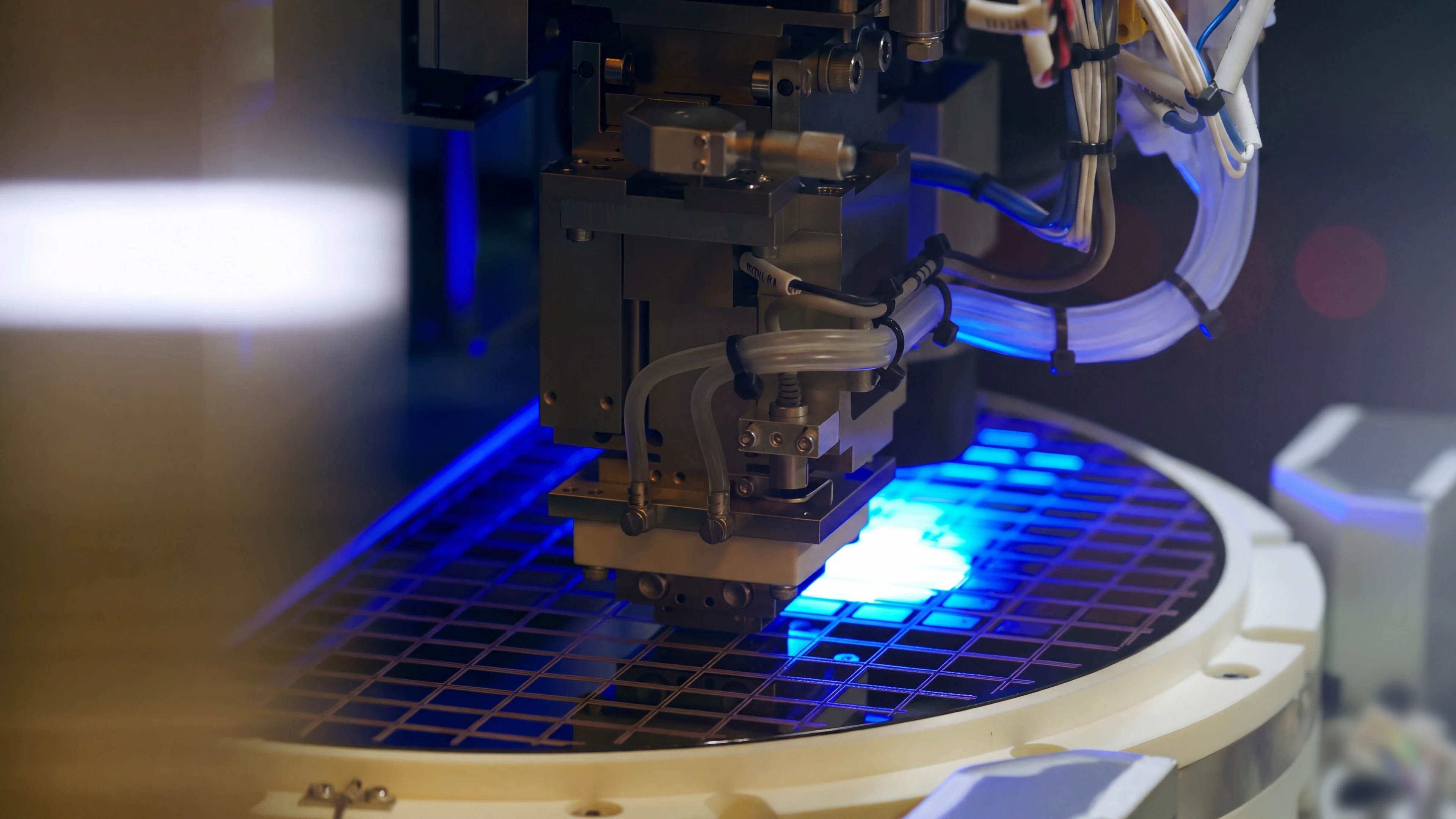
Interfacial precision for advanced semiconductor packaging
Resolving fine-pitch stress in heterogeneous integration. Breaking thermal and conductive bottlenecks for AI chips and core equipment.
AEC-Q100 qualified for extreme thermal shock and aging. A rock-solid physical foundation for SiC/GaN power modules and ADAS compute.
Shattering polymer thermal limits. Robust bonding under cryogenic and extreme-heat cycling, with zero carbonization, embrittlement, or delamination.
Target-engineered for high-end optics, aerospace, and MEMS. Low CTE, shrinkage, and outgassing for micron-level precision fluid dispensing.
Modulus Integrity
Engineered for military sensors and high-power density modules. Tuned via multidimensional rheology to deliver absolute modulus support in extreme environments.
Spectral Transfer
Focused on full-spectrum microelectronic thermal applications. Overcoming conventional adhesion barriers to ensure enduring, high-strength bonding under extreme thermal cycling.
Cohesive Strength
Micro-architected with high-purity nano-silver. Achieving ultra-low volume resistivity and high Tg characteristics, perfectly tailored for fine-pitch printing and precision dispensing.
Decoding material causality through failure physics and first principles.
The difference is not the name on the formulation but the shape of the temperature profile. A duty cycle that only exercises the cold end and tops out a little above 100 °C belongs to a low-temperature adhesive, which can spend its entire design margin on chain-segment freedom and fracture toughness without reserving bond-energy headroom for a hot crosslinked network. A duty cycle that stays above 150 °C and rarely sees deep cold belongs to a high-temperature adhesive, where the focus is oxidation stability, high-temperature modulus and outgassing control. A wide-temperature adhesive has to handle a single interface pulled from both ends: the cold end wants a flat modulus and ample toughness, the hot end wants a rigid, shrinkage-controlled network, and the two orientations are opposite, so the only place to find a joint feasible region is the middle of the profile. If a device pushes against the material boundary at both ends, review it as a wide-temperature adhesive; if one end is effectively idle, a narrow-band product will usually take the metrics further.
These three architectures tighten three constraints inside the same window. HBM4 widens the interface to 2048-bit and moves the base die to a 4 nm logic process, and shipping parts already run from the JEDEC baseline of 8 Gbps to 11.7 Gbps, putting per-stack bandwidth in the 3.3 TB/s range. More than 20,000 through-silicon vias and 16,000 bottom micro-bumps per stack couple memory and logic chiplets more tightly than before, so underfill has to combine low CTE with low-modulus damping inside thinner gaps. CoWoS-class packages keep scaling in area, and once area grows, warpage stops being a secondary concern and becomes a first-order constraint, so underfill and die-attach layers have to hold both void rate and residual stress across a large area. Glass-core substrates change the interface chemistry outright. Glass is smooth and bonds weakly to metal, and metallization inside sub-10 μm through-glass vias plus nanometer-level flatness across large panels are still being worked through, so the material has to balance interfacial coupling, low shrinkage and low outgassing.
Separate the failure path before touching parameters. Damp heat attacks on three lines at once: interfacial hydrolysis and peeling, plasticization that pulls Tg down, and electrochemical migration of mobile ions under bias. If delamination advances along the interface, re-check water absorption, cure shrinkage and the silane-coupled interface first. If leakage current and surface insulation resistance (SIR) degrade first, move to mobile-ion content (Cl⁻, K⁺) and volume-resistivity retention. If popcorn cracking appears after reflow, compare the saturated wet Tg by DMA against the process temperature. The three paths call for completely different formulation changes; running them out of order wastes a qualification cycle.