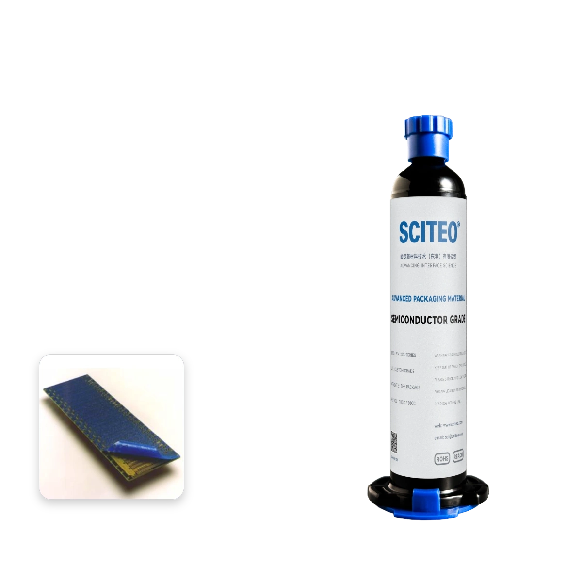
SC6301 Temporary Bonding Adhesive — Semiconductor-Grade, 280 °C PVD/CVD, Acid/Alkali pH1-13, Peel-Clean Removal
Temporary bonding series. 280 °C reflow/PVD/CVD compatible. pH 1–13 acid/alkali 60-min. Low modulus, high elongation, elastic peel-clean removal. Multiple viscosities.
Semiconductor process, PVD/CVD, wet-process plating, chips, PCBA and wafers — temporary protection, masking and bonding.
- Tensile Modulus
- 2–14 MPa
- Temperature Range
- −45 °C–280 °C
- Cure Condition
- UV-cure 5 s
- Elongation at Break
- 210–300 %
SCITEO Rigorous Standards: Qualified under GJB 150 environmental reliability testing by Zhenhua, CETC, and CAC, delivering mission-critical reliability.
Engineered as high-reliability domestic qualified alternatives for semiconductor and defense manufacturing clusters across Shanghai Zhangjiang, Xi'an, Chengdu, and Wuxi.
Specifications Don't Match Your Operating Conditions?
Only the baseline series is shown here. SCITEO's undisclosed archive holds formulations engineered for extreme environments. Contact us — our application engineers will match you precisely.
High Reliability Scenarios
Core positioning and partial application demonstration of this product under complex operating conditions.
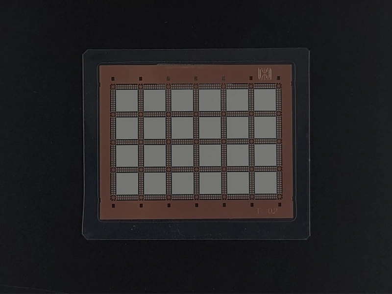
Wafer Fab Masking
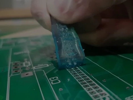
Temporary PCBA Bonding
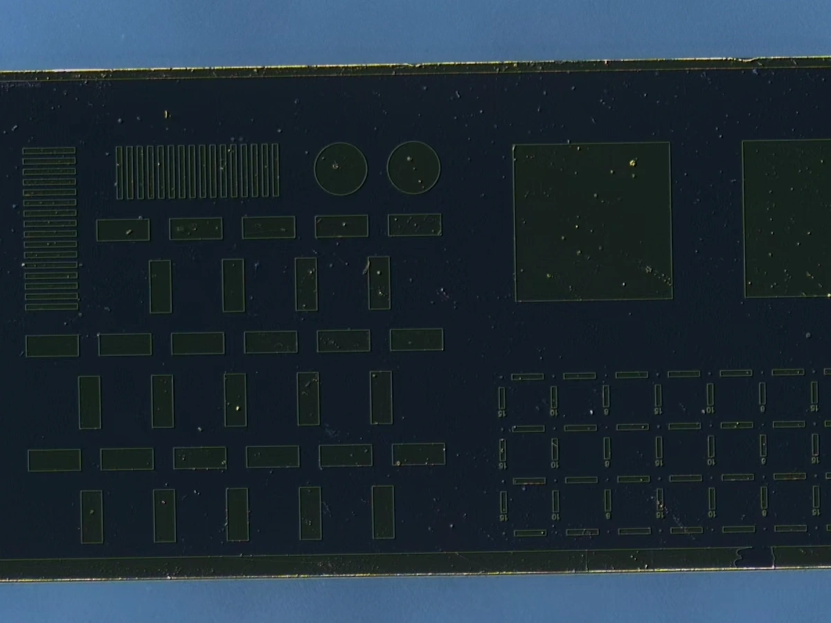
Wafer Fab Fixture Protection
Application Engineer FAQ
A structured brief from SCITEO covering physical properties, application standards, and related specifications.
How does SC6301 protect chip surface patterns during PVD/CVD and strong acid/alkali etching?
A dense hydrophobic barrier with strong interfacial anchoring withstands PVD transient heat at very low outgassing; there is no edge undercut across pH 1–13 wet cycles, and specific polar solvents give high-cohesion sheet peel-off.
Why no thermal degradation through multiple reflow passes? How is residue-free removal achieved?
The series offers over 285 °C of short-term thermal headroom: after repeated lead-free reflow shocks the backbone neither chars nor embrittles, and 210–300% elongation at very low peel force allows clean removal with precision tweezers.
Request Technical Documentation or Consult an Application Engineer
Receive product documentation and customized formulations. Please provide accurate information for verification.
Recommended Advanced Materials
Explore more proven SCITEO solutions for other critical application environments to close the loop on microelectronics safety.
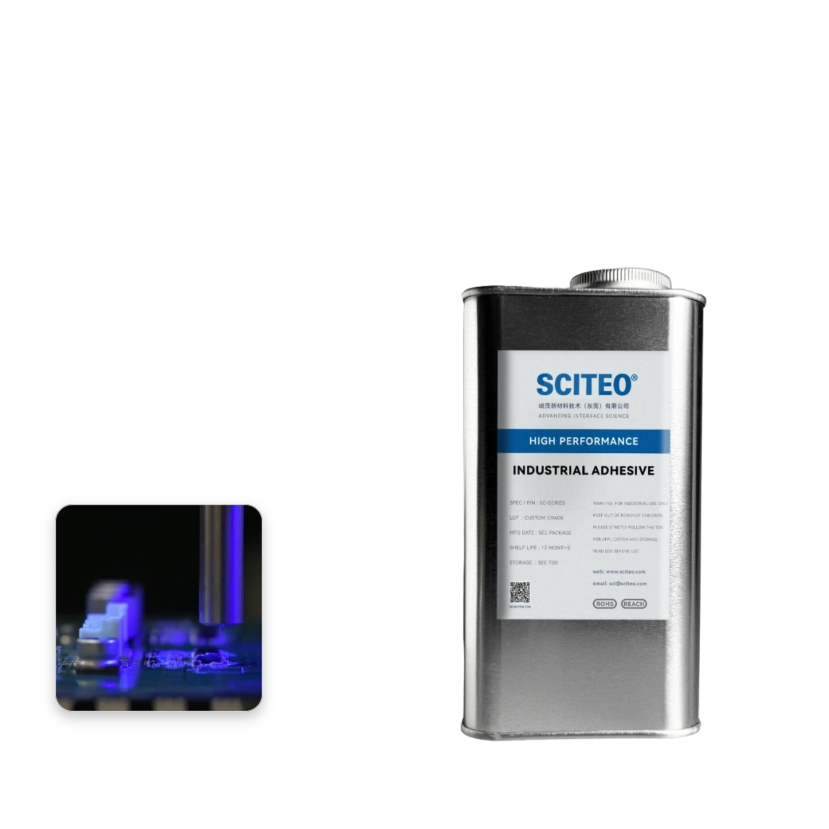
SC9132 Insulating Conformal Coating — PCBA Wide-Temp, Anti-Aging, Chemical-Resistant, Fluorescent Protective Coating
Conformal coating series. PU, silicone, acrylic, UV-cure variants. Wide-temp, chemical-resistant, 85/85 200 h. RT or heat-cure with fluorescent visual identification.
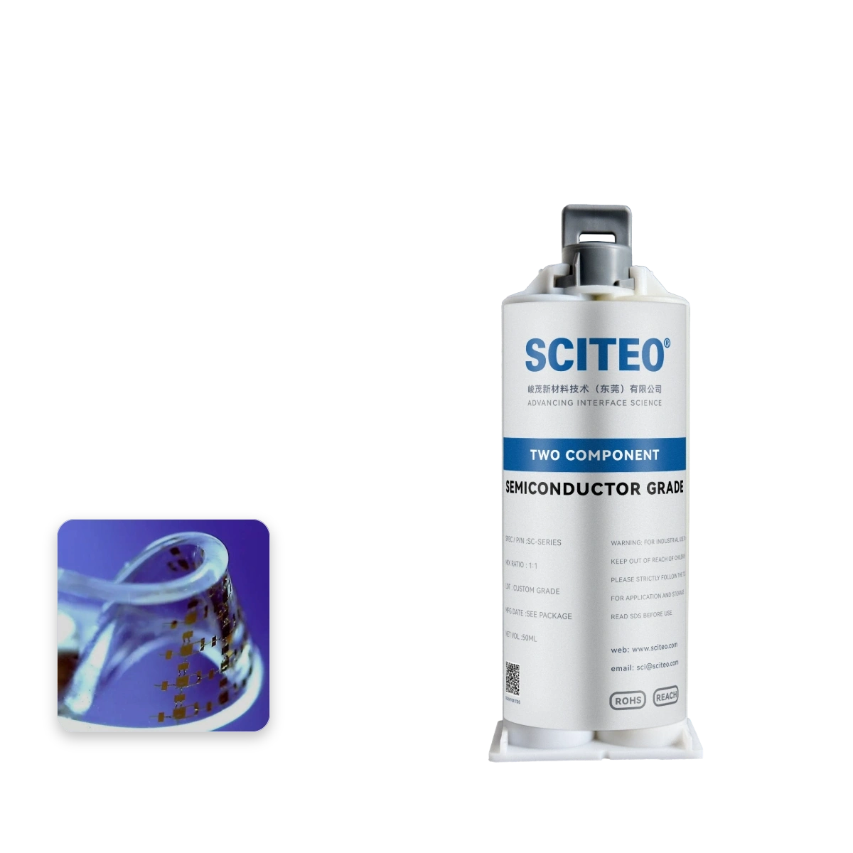
SC609 Flexible High-Transparency PU — Two-Component, RT-Cure, High Elongation, Bonding, Sealing, Anti-Aging
Flexible, high-peel-strength PU. Crystal-clear, high tensile elongation. RT-cure, chemical-resistant, humidity/heat aging. 34 kV/mm dielectric strength. Bonds plastics, glass, metal.
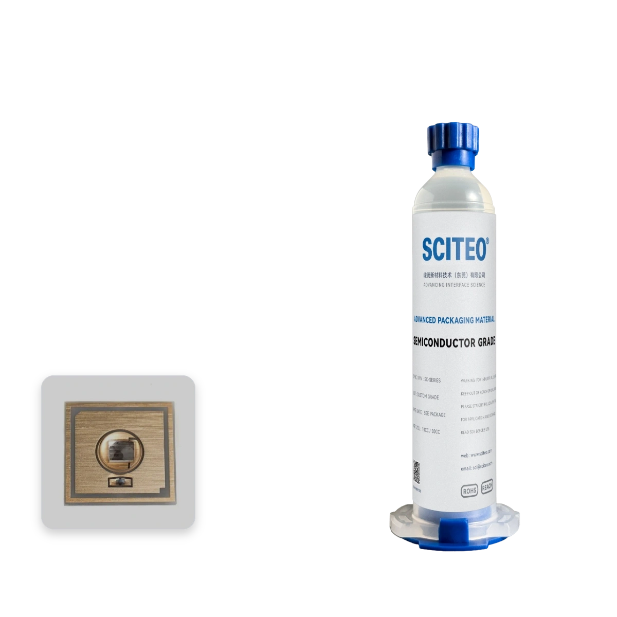
SC6630 300 °C Transparent Epoxy — Single-Component, High-Strength, Insulating, Rigid Bonding & Sealing
Transparent single-component, ready-to-use. Heat-cure for high bond strength, insulating, 300 °C, multi-reflow resistant. Dispensable & printable. 95% shear retention after 1500 h at 190 °C; 500 thermal cycles (−40 to 125 °C): 80% shear retention; damp-heat 1000 h (85 °C / 85% RH): 72% shear retention.