How to Select Underfill: Void & Warpage Control from Chip-Level Packaging to Glass-Based Carriers
From chip-level gaps to CoWoS-class packages and glass carriers, SCITEO frames the joint criteria for voids, warpage and interfacial adhesion
Executive Summary
Underfill yield now turns on the joint optimum of low CTE, high Tg, high thermal conductivity and void control — and no single parameter pushed to its limit holds up a kilowatt-class package on its own.
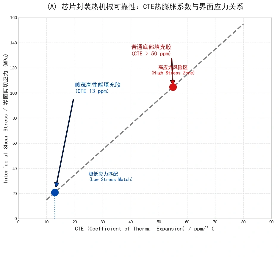
Generative AI training and inference have pushed the bottleneck of compute silicon away from transistor density and into the interconnect density and thermo-mechanical limits inside the package. CoWoS-class 2.5D platforms place logic dies and multiple HBM stacks side by side, micro-bump pitch is collapsing from tens of microns toward 5 μm, and single-accelerator TDP has crossed the kilowatt line. Underfill has moved from a filler material to a structural material that decides yield and service life. Its acceptance criteria are no longer flow and fill alone, but the joint optimum of void rate, interfacial stress, warpage and long-term thermal cycling life. SCITEO combines CTE 13 ppm/°C, Tg 150 °C, 6 W/m·K and 32 MPa into one formulation platform that spans the full scale axis, from chip-level gaps to panel-level glass carriers, turning each segment's constraints into criteria and process windows a customer can verify.
Key Parameter Comparison
The table below places SCITEO underfill grades against conventional auxiliary adhesives so engineering teams can locate the gap during design review:
| Parameter | SCITEO | Industry Norm | Test Standard |
|---|---|---|---|
| CTE (below Tg) | 13 ppm/°C | 30 to 50 ppm/°C | TMA |
| Tg | 150 °C | 80 to 120 °C | DMA |
| Thermal conductivity | 6 W/m·K | 0.2 to 1.0 W/m·K | ASTM D5470 |
| Shear strength | 32 MPa | 10 to 15 MPa | GB/T 7124 |
| Mobile ion content | below 10 ppm | 30 to 100 ppm | Ion chromatography |
| Cure shrinkage | below 0.5% | 1.0% to 1.5% | Density method |
The Underfill Mandate: Advanced Packaging Turns an Auxiliary into a Structural Material
The industry's performance narrative has shifted from shrinking transistors to stacking dies at high density. A single-exposure reticle field tops out near 26 mm × 33 mm (about 850 mm²), and pushing a monolithic die past that ceiling degrades yield nonlinearly with area. The industry therefore splits designs into chiplets and reassembles compute, memory and I/O dies from different process nodes inside one package. That route solves yield first and bandwidth second, and both eventually land on the interface materials: being able to assemble a package does not mean it stays assembled through years of thermal cycling.
Large-Format 2.5D: Local Silicon Bridges Take the Lead
The backbone of CoWoS-class 2.5D integration has shifted from a full silicon interposer (CoWoS-S) and a redistribution-layer (RDL) interposer (CoWoS-R) toward CoWoS-L, which embeds local silicon interconnect (LSI) bridges in an organic carrier: local high-density interconnect buys low warpage at large format, which is why it has become the volume route for large AI accelerators. Interposer formats have moved from the 3.5-reticle generation to 5.5-reticle, with more HBM stacks mounted alongside. Every step up in package area multiplies the interfaces and scales CTE mismatch with them, so the tolerance left to any single interface is razor-thin — one layer sitting off its intended expansion is enough to show up as visible warpage or delamination.
That is the dividing line in the role of underfill. In a conventional flip-chip package its job is to fill between solder bumps and spread stress. In a large 2.5D package it also participates in warpage control and in defining the heat path, which makes it a third structural layer alongside the die and the substrate.
Three Constraints Tightening at Once
Three constraints are tightening inside the same window. The most direct one is the gap: micro-bump pitch is contracting from the 40 μm range toward 10 μm and below, the industry has already placed bonding and underfill solutions for roughly 5 μm bumps on its development list, and the effective hydraulic radius of the capillary channel shrinks with it. The second is the temperature gradient: single-accelerator TDP now runs 1.5 kW to 2.5 kW, rack power has crossed 200 kW and is heading for the megawatt class, power delivery is moving to 800 V high-voltage DC, and cold plates remove heat from the lid while widening the gradient between die and lid. The third is format: large packages warp more readily through reflow and thermal cycling, and once an interface delaminates, stress is immediately redistributed onto the solder joint root.
The intersection of these constraints is the engineering window for underfill. It must complete a void-free fill through a gap of tens of microns or less, then isolate the solder joints from shear stress through low CTE, high Tg and adequate strength. No single metric is hard to push to its limit; the difficulty is that they constrain one another inside a single formulation, so selection can only land on a joint optimum.
Failure Mechanisms: Underfill Has to Hold Stress, Voids, Ions and Heat Paths at Once
Silicon has a CTE of about 2.6 ppm/°C and organic substrates about 15 to 20 ppm/°C, with silicon interposers and glass carriers sitting between them. A package sees a 260 °C lead-free reflow peak and then cools to room temperature, and the mismatch in contraction accumulates into substantial shear stress. Without intervention the first failure usually appears at the micro-bumps along the die edge, because less solder volume means less plastic strain capacity and earlier fatigue crack initiation under the same strain.
Stress Redistribution: Spreading Load from the Joint to the Interface
Underfill is dispensed along the die edge, wicks into the bump array by capillary action, and cures into a high-modulus crosslinked network that spreads the shear stress concentrated on solder joints across the die-to-substrate interface, returning the joints to their job as conductive channels. In mobile and automotive modules the same layer also absorbs dynamic mechanical stress from drop and vibration, which raises board-level cycling life measurably.
More modulus is not automatically better. Excessive modulus transfers stress into fragile low-k dielectric layers and ultra-thin dies, while insufficient modulus cannot hold structural rigidity through thermal cycling. The 8 to 11 GPa storage modulus band has been repeatedly validated in advanced packaging because it is the balance point between stress transfer and structural support. For ultra-thin stacked dies, choosing a low-modulus grade to absorb thermo-mechanical mismatch is equally common, and the trade-off follows the load path of the package. SCITEO builds storage modulus into a multi-grade platform, so packages with different load paths can each take the value they need.
Zero Voids: Position Matters More Than Count
Voids are the leading cause of underfill failure, but the judgment should weigh position at least as heavily as area fraction. A void sitting at the solder joint root or in an interconnect channel cuts the thermal and electrical path directly, whereas an isolated micro-void at the edge is often only a sign that the process sits near the edge of its window. Following the IPC-7095 logic, area fraction and position have to be evaluated together before a line is stopped for rework — a single total void rate misses the real risk. Inside its production window, SCITEO holds void area fraction within 1% and keeps voids off solder-joint roots and interconnect channels; after 1,000 cycles from −50 to 125 °C, void area fraction grows by less than 0.5%, with no new voids at joint roots.
Rework reviews quantify before they attribute: confirm area fraction and position, then trace the dominant cause. Voids scattered along the substrate edge point to entrapped gas from insufficient preheat; voids strung along the converging flow front point to a dispense path that seals the vent before the fill completes; voids clustered at the pads point to flux residue that changes local surface tension and blocks wetting. At a 5 μm bump pitch all three are amplified at once, and flux cleaning and residue control decide whether the process scales. The physics is the same as the cleanliness demand in hybrid bonding, except underfill faces a mixed organic and inorganic interface with a narrower process window.
Sealing and the Ion Barrier
Micro-gaps inside a package are pathways for moisture and ion migration. The cured underfill layer has to form a continuous sealing interface that blocks the moisture path and prevents electrochemical migration from degrading insulation under bias. The quantitative metric is mobile ion content, typically controlled for Na⁺ and Cl⁻ by ion chromatography. For automotive and industrial modules that serve in hot and humid conditions, ion content and moisture absorption often decide service life more than initial strength — strength degrades gradually, insulation failure is abrupt.
Auxiliary Heat Conduction
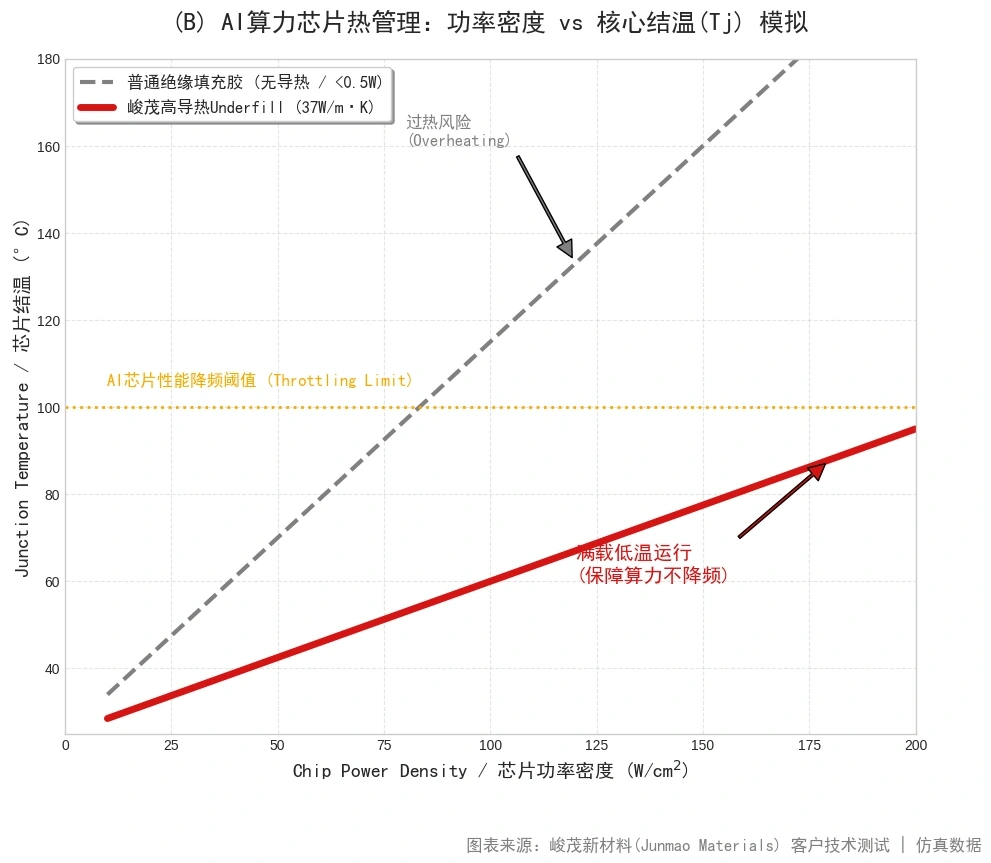
In a high power-density package the space between bumps is a poor thermal path. A thermally conductive underfill turns that space into a low-resistance route, which lowers junction temperature and spreads hotspots when combined with the main path through the lid and cold plate. Thermal design trends keep raising the value of this capability. Once accelerator power passes the kilowatt mark, air cooling is progressively ruled out and direct-to-chip liquid cooling becomes the baseline, which makes interfacial thermal resistance one of the variables that decide whether sustained compute throttles. When a single package carries both a high-power compute die and temperature-sensitive memory stacks, flattening the heat flow without creating a new hotspot is often more effective than raising local conductivity alone. SCITEO thermally conductive underfill targets exactly that segment — turning the space between bumps from a thermal bottleneck into a heat path.
The Parameter Boundaries of SCITEO Underfill
SCITEO develops multiple epoxy-based fill series for different process requirements, covering insulating, thermally conductive and high-temperature directions. Four metrics define the selection boundary for large-accelerator packaging and frame the trade-off logic of the SCITEO formulation platform.
CTE: Converging on the Combined Expansion of Silicon and Substrate
Warpage is the primary risk in large packages, and its source is accumulated CTE difference across layers as temperature changes. SCITEO raises filler loading with micro and nano silica to bring CTE down to 13 ppm/°C, converging on the combined expansion of the silicon die and the organic substrate. The effect on joint life is an order of magnitude: the closer the CTE sits to the bonded materials, the lower the interfacial shear stress under thermal cycling, and the later fatigue cracks initiate.
Lowering CTE raises viscosity in return. Every step up in filler volume fraction increases capillary flow resistance, so CTE and flowability must be evaluated inside the same process window rather than optimized separately. That is also why high-loading systems require particle size distribution design rather than simply adding more filler.
Tg and Modulus: Holding Rigidity Across the Load Range
The glass transition temperature determines the point above which the material loses rigidity. SCITEO high-Tg underfill reaches a Tg of 150 °C, well above the junction temperature range of a fully loaded accelerator, which means the material stays in the glassy state and keeps supporting the joints instead of softening and collapsing. For accelerators that run at high load for long periods, this directly governs whether joint fatigue life stays inside its design range.
Tg and CTE must be evaluated as a pair; isolating either one hides the actual failure order. CTE mismatch against silicon lets shear strain accumulate through every thermal cycle, so the interface cracks before strength metrics give way. CTE match with insufficient Tg lets the modulus step rewrite the stress distribution inside the operating range, re-routing the load path and turning the joints from a protected zone into the new load-bearing line.
Thermal Conduction: Balancing Flow Against Heat Transfer
High thermal conductivity is normally achieved by raising ceramic filler content, which simultaneously raises viscosity, CTE and brittleness. SCITEO thermally conductive underfill reaches 6 W/m·K — roughly ten times the 0.2 to 1.0 W/m·K of conventional underfill — while retaining flowable low-viscosity behavior, so heat transfer improves without sacrificing capillary penetration. That balance line has to be calibrated repeatedly in the lab: a small shift in filler system or particle size distribution trades flowability against conduction, and capillary fill time on the line moves with it. Selection therefore has to rest on measured data.
The test conditions themselves change the answer. Underfill thermal conductivity is highly sensitive to pressure and bond line thickness (BLT) — a thinner BLT packs the filler network closer to continuity and reads higher — and the spread between samples often exceeds the difference between formulations. Design reviews should fix pressure and BLT before comparing, and treat interfacial thermal resistance, not bulk conductivity, as the final criterion across candidate materials.
Bond Strength and Low Ion Content
Underfill is usually classified as a non-structural adhesive, yet large dies generate substantial peel load at the interface under thermal cycling, and weak strength means delamination precedes joint fatigue. SCITEO formulations reach 32 MPa shear strength while retaining flowability, above the 10 to 15 MPa typical of comparable products. Combined with low ion content and low cure shrinkage, the interface holds up better under the combined action of damp heat and thermal cycling.
SCITEO Formulation Matrix: Selection Logic Along the Packaging Scale
Underfill selection reduces to three physical quantities: gap height sets the dynamic window of capillary flow, package area sets how much CTE mismatch accumulates, and takt time sets how much process margin is left. The three trade off along the packaging scale — the narrower the gap, the tighter the flow window; the larger the carrier, the less stress margin is left per layer; the faster the takt, the less room the process has to adjust. SCITEO organizes its formulation matrix along that axis, so every segment maps to material actions a customer can verify.
Small Gaps and Fast Takt: Flow Windows for CSP, SiP and Flip Chip
Chip-level packaging has pushed bump standoff down to 20 to 50 μm, and the material must deliver low viscosity, fast flow and zero flash inside that window, which makes it the narrowest process window on the scale. Flip chip and wafer-level chip-scale standoffs sit an order of magnitude below conventional BGA, and viscosity at dispense temperature usually has to land in the 300 to 500 mPa·s range for void-free penetration. Temperature at both the dispense and the substrate side therefore becomes the governing variable: substrate preheat moves the material into a low-viscosity range the moment it touches the board, with 40 °C to 80 °C common for gaps around 30 μm, while fine-pitch flip chip lines push toward 100 °C and hold the needle at temperature to shorten fill travel time. Higher is not better — excessive heat gels the material before the cavity is full and vaporizes volatile fractions into bubbles — so low-stress formulations pair a staged ramp of 2 to 3 °C/min with a multi-stage cure, completing flow at lower temperature before raising temperature to build the crosslinked network.
SiP and multi-die packaging raise the difficulty another step. Logic, memory, power management and RF dies sit side by side on one substrate with inter-die gaps as narrow as 100 μm, and each die differs in size, gap and surrounding structure, so a single substrate often needs two or more dispensing paths. The substrate also sits next to bond pads, optical apertures and RF traces, where any underfill flash is an immediate functional failure, which makes dispensing accuracy and keep-out zone control as important as the material itself. Takt time is equally demanding: advanced lines target below 10 seconds per substrate, which is why non-contact jet dispensing has become the mainstream choice — it removes needle Z travel while holding each shot in the sub-milligram range. SCITEO supplies a range of viscosity and flowability grades at this segment, covering the gap range from flip chip to SiP modules, and pairs multi-stage cure with low-CTE formulations to limit cure warpage.
Large Format and Fine Pitch: Warpage and Void Control in CoWoS-Class Packages
Once the package scales up, interfaces multiply and the stress tolerance left to any single layer is squeezed with them. Accelerator packages have moved into the 60 mm to 100 mm and larger range, with solder counts running from several thousand to tens of thousands, pitches narrowing to 0.4 to 0.8 mm, and per-package power in the kilowatt range. A package sees a 260 °C lead-free reflow peak and then cools to room temperature, and the difference in contraction between silicon and the organic substrate accumulates across the full footprint, showing up as corner lift or center bow. Once warpage exceeds the coplanarity tolerance of the solder balls, it produces soldering defects that functional test rarely exposes. Underfill turns the micro-bumps from load-bearing members into conductive channels and spreads the interfacial stress through its own contraction behavior.
With HBM4 the interface doubles to 2,048 bits and stack height continues toward 16 layers. JEDEC raised the package height limit in JESD270-4 from 720 μm to 775 μm, and the extra 55 μm returned microbump routes to the viable zone — which is why leading memory makers continue to run thermal compression bonding (TCB) with mass reflow molded underfill (MR-MUF) as the backbone process, packing thinner dies and smaller inter-layer gaps into one thickness budget. The core problem this structure poses is coupled shrinkage: a stack built from thin dies and molding compound hangs off a silicon interposer and an organic substrate, so any CTE deviation in any layer accumulates into warpage at the interposer edge. SCITEO holds CTE at 13 ppm/°C, raises Tg to 150 °C, and tightens cure shrinkage so that the underfill contracts in step with the stack through the cooling segment of the cure. Cure shrinkage is the first-order variable here, because it decides whether residual cure stress opens the fragile low-k structure; on molded underfill routes the shrinkage of the molding compound and of the underfill must also be checked against the same curve, or the difference becomes a new stress concentration at the inter-layer interface.
Fine-pitch bumps push the same segment to its limit. In the latest supply-chain reports, a leading foundry has asked its materials and equipment partners to develop bonding and underfill solutions for roughly 5 μm-class micro-bumps rather than move the HBM-to-interposer interface to copper hybrid bonding; the industry consensus is that quality assurance below 15 μm remains difficult, and the harder problem is the underfill that can guarantee a void-free fill at that gap — not the bumps themselves. At 5 μm the effective capillary radius is extremely small, and void-free filling, flux residue removal and alignment consistency must all be solved together, with a single miss multiplying through yield. SCITEO shifts the formulation focus at this scale from simply lowering viscosity to reshaping the flow front. Multimodal grading of sub-micron spherical fillers lowers the packing resistance of filler under shear, and surface-modified wetting control keeps the front advancing continuously through a narrow gap instead of jumping intermittently. Low-alpha, high-purity fillers control soft error risk, and mobile ion content is held low. For modules with an explicit rework requirement, the right choice is a grade that softens at the target temperature, with post-rework void assessment and boundary-scan verification written into the process specification.
Large-Carrier Fill: Fill Time and Interfacial Adhesion After Area Scaling
Once the carrier grows, the dominant problem shifts from getting material in to getting it in evenly — wafer-level packaging moves the carrier to a 200 mm or 300 mm wafer, and panel-level packaging (PLP) replaces it with a rectangular panel. Along a single dispense path, flow distance stretches with carrier format, so capillary fill time and dispensed volume distribution become ever harder to keep consistent — the window left to the material is only the stretch before gelation — and the warpage level of the reconstituted carrier directly affects the alignment accuracy of the redistribution layers built on top of it. SCITEO underfill grades for this direction pair multiple viscosity options with high-speed dispensing windows, holding fill time inside the gelation window and using low-shrinkage formulations to limit carrier-level warpage.
Glass-based carriers are the second branch of this route. Glass is chemically inert, conventional coupling systems struggle to form stable bonds, and the interface between a through-glass via (TGV) and copper tends to lose adhesion after high-temperature processing — the first failure an underfill exposes on a glass carrier, and not a matter of peak adhesion being too low. SCITEO establishes reliable adhesion between glass and copper through interfacial coupling and wetting control, and verifies that the bond neither delaminates nor outgasses after high-temperature processing. On a large carrier, adhesion uniformity matters more than peak adhesion: a single local weak point becomes the origin of whole-area failure in later thinning or thermal cycling.
Cross-Scale Validation: Co-Packaged Optics and a System-Level Criteria Loop
Returning underfill to the finished system, the most demanding test bed is co-packaged optics (CPO). Once the optical engine and the switch ASIC share one substrate, sub-micron optical alignment tolerance becomes something the underfill layer has to underwrite: shrinkage during the cooling segment of the cure pulls the coupling position off its design point, while the optical engine can neither absorb rigidly transmitted stress nor tolerate an interface that loosens through thermal cycling. Low shrinkage and low modulus stop being two independent specs and become a pair of constraints pulling against each other, and the formulation has to satisfy both at once. This route has moved past proof of concept, with co-packaged optics Ethernet switches in volume production, and the heterogeneous integration of optical engine and ASIC pushing PIC/EIC alignment, CTE mismatch and optical port cleanliness onto the material together; SCITEO's reserved low-shrinkage, low-modulus stress-buffering direction for co-packaged optics and high-speed optical modules targets exactly that pair.
Conditions like these also bring the validation method forward. No single parameter or one-off test represents field performance: thermal conductivity has to be converted into interfacial thermal resistance at the target pressure and thickness, voids have to be judged on area fraction and position together, and bond strength has to be re-measured after thermal cycling and damp heat. SCITEO aligns these three criteria with customers at the design review, so that a selection conclusion can be reused across scales instead of triggering a fresh trial-and-error cycle for every package format.
Selection Criteria at a Glance
The tables below compress the mechanisms above into executable selection criteria anchored to each segment of the packaging scale, for direct use in design review.
The first table maps scale range to failure mode and criterion:
| Scale Range | Typical Failure | Key Criteria | SCITEO Direction |
|---|---|---|---|
| Small gaps and fast takt (flip chip, CSP, SiP) | Voids, flash, contamination of adjacent structures | Substrate preheat window, viscosity grading, keep-out zone control | Multi-viscosity underfill series |
| Large format and fine pitch (CoWoS-L class packages) | Warpage, interfacial delamination, joint fatigue | Cure shrinkage, modulus and CTE matching | Low-stress high-Tg underfill |
| Stacked and molded underfill (HBM, MUF/MR-MUF) | Inter-layer delamination, thermal resistance drift | Filler grading, flow front stability | Thermally conductive underfill (6 W/m·K) |
| Large-carrier fill (wafer level, panel level and glass carriers) | Incomplete fill over large area, carrier warpage, throughput limits | Capillary fill time, dispense window, low shrinkage | High-flowability low-shrinkage underfill series |
| Cross-scale validation (co-packaged optics and high-speed optical modules) | Coupling position drift | Low shrinkage, low modulus | Low-stress optical packaging formulation |
The second table converts key metrics into acceptance criteria:
| Acceptance Item | Recommended Criterion | Verification Tool |
|---|---|---|
| Voids | Area fraction and position evaluated together | Acoustic scanning (C-SAM), IPC-7095 |
| Interfacial stress | No delamination after thermal cycling | JEDEC JESD22-A104 |
| Thermal resistance | Interfacial resistance at target pressure and thickness | ASTM D5470 |
| Ionic contamination | Mobile ions below 10 ppm | Ion chromatography |
| Warpage | Residual warpage controllable on large packages | Shadow moiré, TMA |
Conclusion: From Parameters to Yield
The value of underfill has never been written on a single parameter. CTE, Tg, modulus, viscosity and thermal conductivity genuinely constrain one another, and what decides yield is their joint optimum inside one formulation plus the ability to reproduce it inside a specific dispense and cure window. From chip-level modules to glass carriers, the number of interfaces is rising, the format is growing and the temperature range is widening, so the tolerance left to materials keeps thinning. SCITEO operates as an integrated R&D and volume manufacturer of high-end materials and keeps investing in low-CTE, high-Tg, high-conductivity and low-stress formulation platforms, turning stress management, heat conduction and cleanliness control into engineering criteria that customers can verify.
This article is SCITEO Advanced Materials original technical content; unauthorized reproduction is prohibited.
Appendix: Process & Engineering Adhesive FAQ Index
How do I select the right underfill viscosity?
Viscosity is set by bump pitch and chip-to-substrate gap height: the smaller the gap, the lower the viscosity required. Fine-pitch packages below 40 μm need a low-viscosity grade for smooth capillary flow, and 5 μm bumps compress the usable viscosity window further. SCITEO offers multiple viscosity and flowability grades; selection should follow capillary fill time and flow front stability at the target gap rather than a single viscosity value.
What are SCITEO underfill curing conditions and the recommended profile?
Step curing is recommended to limit the thermal stress introduced during cure. The specific profile is customized to die size, stack count and substrate material, typically staged between 100 °C and 150 °C, with the high-Tg network established on completion. For large packages, cure shrinkage and residual warpage should be confirmed in the same review so that contraction mismatch during the cooling segment is captured.
Can underfill be used together with conductive silver adhesive?
Yes. SCITEO runs a full semiconductor process adhesive line, and our underfill and chip-attach conductive silver adhesive are compatibility tested as a set. Both offer low CTE, with underfill down to 13 ppm/°C, and combined use further improves overall module reliability.
Why do voids appear in underfill, and when does a line need rework?
Voids typically come from three sources: insufficient substrate preheat, which degrades flow and entraps gas; a dispense path that lets converging fronts seal the vent early; and flux residue on the pad, which changes local surface tension and blocks wetting. The decision to stop a line depends less on void count than on void location. Voids at the solder joint root or in an interconnect channel cut the thermal and electrical path directly, so area fraction and position should be assessed together per IPC-7095, and the process re-verified after adjusting dispense path, preheat temperature and cleaning.
What makes underfill difficult once bump pitch reaches 5 μm?
At 5 μm the effective capillary radius is extremely small, and void-free filling, flux residue removal and alignment consistency all tighten at the same time — and the industry consensus is that the harder problem is the underfill, not the bump, with quality assurance below 15 μm still difficult. On the material side, viscosity must stay low while the flow front is reshaped. This usually relies on multimodal grading of sub-micron spherical fillers to reduce packing resistance under shear plus surface modification for wetting control, while mobile ions and filler impurities are held low so contamination is not amplified inside the narrow gap. SCITEO supplies formulation directions centered on flow front stability for this scale.