PVD/CVD Coating Adhesives: High-Temp and Low-Outgassing Selection Criteria for Wafer Metallization, Optical Coating and Glass Substrate Packaging
SCITEO 300-400 °C low-outgassing bonding, HF-resistant chemistry and zero-residue UV strippable masking across wafer metallization, optical coatings, and glass substrate and panel-level packaging
Abstract
Verdict first: the yield floor of a PVD/CVD line is set less by the coating tool's base vacuum than by the auxiliary bonding and masking materials that ride into the chamber with the workpiece. Four requirements settle the selection: CVCM below 0.1%, which holds the chamber cleanliness floor; long-term endurance above 300 °C, which covers the combined heat load of substrate preheating and plasma bombardment; no undercut in HF mixed acid or strong base; and a 0% residue peel.
Physical vapor deposition (PVD) and chemical vapor deposition (CVD) do the surface engineering inside the vacuum chamber — wafer metallization, optical thin films and lens coatings, power-device seed and barrier layers — and the application base keeps expanding into glass substrates and panel-level packaging. Across all of it, the demands on auxiliary materials converge on one set of physical quantities: extremely low condensable volatiles, thermal margin against plasma bombardment and radiant heat, chemical inertness to etchants, and interface cleanliness after peel.
This article crosses vacuum physics, thermodynamics and wet pre-/post-treatment chemistry to dissect how auxiliary materials fail along the PVD/CVD chain, then reduces that to criteria a process engineer can execute directly. SCITEO Advanced Materials supports those four with first-party outgassing data and rheology design across wafer metallization, optical coatings, glass substrates and panel-level packaging.
Core Parameter Comparison
The table below compares SCITEO PVD/CVD adhesives with conventional auxiliary adhesives:
| Parameter | SCITEO | Industry Standard | Test Method |
|---|---|---|---|
| Long-term temperature limit | 300-400 °C | 150-200 °C | TGA / long-term heat aging |
| 5% weight-loss temperature (Td5) | 465 °C | 310 °C | TGA |
| Continuous rating at 400 °C | 72 h+ stable | Carbonized | High-temperature bake |
| CVCM condensable volatiles | below 0.1% | above 1% | ASTM E595 |
| Water absorption (ultrasonic cleaning) | below 0.03% | above 0.5% | GB/T 1034 |
| PVD coating shear strength | 20-30 MPa | 2-5 MPa | GB/T 7124 |
| Thermal conductivity range | 4-60 W/m·K | 1-3 W/m·K | ASTM D5470 |
| Strippable mask elongation at break | above 300% | below 50% | ASTM D412 |
| UV cure time | 3-5 s | above 30 s | In-house method |
| Strong polar solvent immersion | 30 days, no anomaly | Swelling or leaching | ASTM D896 |
| Mask peel residue rate | 0% (one-piece peel) | Visible residue | Visual / microscopy |
CVCM and TML are measured under the ASTM E595 baseline of 125 °C, 24 h and no more than 5×10⁻⁵ Torr; aerospace and high-vacuum industries have long used TML 1.0% and CVCM 0.1% as material screening levels. Actual chamber heat load runs far above that baseline, so SCITEO adds a 300 °C tightened retest and reads high-temperature desorption rates against ASTM E1559 outgassing kinetics.
The Defect Spectrum of PVD/CVD Vacuum Processes
The four most frequent anomalies on a coating floor get logged under four different causes and trace back to one variable: the auxiliary bonding and masking materials that enter the chamber with the workpiece. None of them show up on an equipment checklist or in the recipe parameter table.
Vacuum Stalling and Target Poisoning
Before sputtering starts, the chamber has to pump down to an ultimate base vacuum in the 10⁻⁵ Torr range. The classic symptom is pumps at full load while the vacuum plateaus. The same batch may also show target oxidation or poisoning: sputter rate collapses, films come out dark, and transmittance and sheet resistance drift together. When equipment-side checks come back clean, the root cause is often the adhesive that rode in with the workpiece — evolved organics condense on target and substrate and build a dense hydrocarbon barrier layer. Pump-down curves plus residual gas analysis (RGA) make the case: when the water peak and the hydrocarbon peak rise together, the auxiliary material is the prime suspect.
Poor Film Adhesion, Micro-Cracking and Peeling
Deposition typically runs between 200-400 °C, and substrate and nascent film exchange heat through ramp, soak and cooldown. Micro-cracks at the film edge after cooldown and a full tear-off in a cross-hatch adhesion test are two readings of one causal chain: interfacial thermal stress has no release path, and the substrate surface has already lost its active sites to organic residue, so the film finds no true chemical bond.
Pre-Cleaning Swelling and Post-Etch Side-Leakage
Coating sits in the middle of the wet process. Upstream is strong-alkali degreasing and ultrasonic acid cleaning (RCA clean and the like); downstream is patterned etching. Masking and temporary-bonding adhesives have to hold their dimensions and their interface across both. Once the cross-linked network is forced open by alkali or mixed acid, etchant undercuts along the seam and the underlying precision circuit or optical microstructure is scrapped within a few cycles.
Mask Flash, Leakage and Residue
Selective PVD, and the lift-off metal patterning that often follows it, both require the non-coated area to be sealed. High-temperature tape and metal fixtures do not conform to 3D surfaces, so edge leakage and flash appear. A liquid masking adhesive that fails cohesively after plasma bombardment breaks apart on peel and leaves microscopic residue that goes on to disrupt lithography, bonding and visual inspection.
Failure Paths of Auxiliary Materials in Vacuum and Chemical Environments
These defects get booked against the equipment: leakage, power drift, target life. Inspection comes back clean, and the problem sits with the auxiliary bonding material inside the chamber — lens-to-frame bonding adhesive, wafer temporary-bonding adhesive, selective masking adhesive — whose failure concentrates in four places.
Vacuum outgassing and target fogging: unreacted monomer and oligomer left in the resin keep desorbing under high vacuum, and desorption rates step up again above 300 °C. The evolved organics offset the pump's effective throughput while condensing on target and substrate as a hydrocarbon barrier layer, after which the film cannot bond and reads as haze. The risk is quantified with total mass loss (TML) and collected volatile condensable materials (CVCM) per ASTM E595.
Delamination from insufficient thermal endurance: unmodified epoxy or acrylate systems soften near 300 °C, then carbonize to powder after backbone scission and lose all grip on the substrate. With no buffer layer to absorb the thermal expansion difference between glass and metal, stress tears the assembly apart. Endurance has to be read together with Td5 — a high headline rating with no margin in between will not survive a single process cycle.
Interface sealing collapse from chemical swelling: ultrasonic alkali, hydrofluoric acid (HF) and strong polar solvents penetrate the free volume of the cross-linked network and force the chains apart. Once the seal fails, cleaning chemistry stays in the interface and etchant follows; molecules released by swelling also condense in the chamber, carrying contamination from the workpiece side over to the equipment side for a second failure mode.
Irreversible residue from cohesive collapse: after plasma bombardment and radiant heat the masking film embrittles and its peel mode shifts from cohesive to interfacial, so the layer breaks on the substrate instead of coming off in one piece. The ghost it leaves converts into particle defects and interface voids in downstream lithography, hybrid bonding or wire bonding, and the later the stage, the harder that residue is to clean.
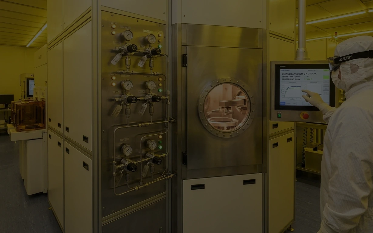
The SCITEO Response: Adhesives Across the PVD/CVD Chain
SCITEO Advanced Materials organizes its formulation platforms around polymer phase transition and high-density cross-linking, matches chemistry to the operating condition, and bases selection on first-party outgassing, chemical-resistance and rheology data.
Automotive LiDAR and Optical Sensor Windows: High-Vacuum Bonding and Ultrasonic Cleaning Resistance
LiDAR windows, infrared windows and optical sensor modules sit in two environments at once — ultrasonic cleaning and high vacuum — which settles two baseline requirements: low water absorption, and no substitution of a short-term temperature rating for long-term endurance.
SCITEO window bonding systems use an electronic-grade purified resin that cures into a high-density network; hydrophobicity holds water absorption below 0.03% in an ultrasonic bath (GB/T 1034). The low-volatile formulation measures CVCM below 0.1% under the ASTM E595 baseline of 125 °C and 24 h, then goes through a 300 °C vacuum retest, so target life and coating quality are protected at the formulation level rather than the equipment level. High modulus builds a stable bond to glass, aluminum alloy and stainless steel, and coordinated modulus and cure shrinkage absorb the expansion difference between quartz and aluminum, keeping the window crack-free through 3 hours at 300 °C.
SiC/GaN CVD Epitaxy and Etch Masking: Strong Acid/Base plus 400 °C Thermal Shock
SiC and GaN epitaxy and etching push auxiliary materials to two limits at once: deposition temperature in the 400 °C class, and chemical attack from upstream RCA alkali clean and downstream HF mixed-acid etch.
The SCITEO specialty high-temperature system holds continuously for more than 72 hours at 400 °C in a high-temperature bake. TGA puts its 5% weight-loss temperature (Td5) at 465 °C with headroom beyond 500 °C, so physical form and interface integrity survive the CVD plasma. On the chemical side, the same system shows no swelling and no leaching after 30 days of continuous immersion in industrial-grade acetone and isopropyl alcohol (IPA) per ASTM D896, holding up to RCA alkali clean and HF etch; a network that does not swell also keeps pre-chamber desorption risk down, which suppresses undercut at the edge by mechanism rather than by process workaround.
High-Power IGBT and Power-Device Substrate PVD Metallization: Anchoring to Low-Surface-Energy Interfaces and Building the Heat Path
A PVD metal layer is dense, low in surface energy, and carries almost no polar groups for chemistry to grab. Conventional thermal adhesives bond to it by physisorption and come off as a whole under vibration or thermal cycling.
The engineering entry point is interface chemistry: specialty silane coupling and polar-group grafting build molecular-level anchoring on inert metal surfaces, reaching 20-30 MPa shear strength (GB/T 7124) with no decay after 30 days in hydrocarbon and 5% salt spray. Thermal conductivity spans a continuous 4-60 W/m·K range (ASTM D5470); grades are picked by heat flux from 4 W/m·K structural bonding up to 60 W/m·K extreme heat spreading, and heat cure completes the thermal path downstream of power-module metallization.
3C Components and Structural Parts: Selective PVD Masking and Clean Peel
3C components and structural parts are where selective PVD runs the highest volume. Phone midframes, foldable-hinge covers, wearable housings and camera decorative rings often carry decorative films (ion-plated black, gradient tones) and functional films (DLC, TiN, CrN, anti-fingerprint) on the same part in separate zones. The substrate spectrum is wide: 6000- and 7000-series aluminum alloys, stainless steel, titanium alloys and magnesium-aluminum alloys, through to specialty substrates such as Kovar (Fe-Ni-Co controlled-expansion alloy) for glass-to-metal seals (GTMS) and hermetic package headers. Kovar's CTE of roughly 5-6 ×10⁻⁶/K matches borosilicate glass and alumina ceramics closely, but it forms a trivalent oxide at room temperature, so acid pickling and anneal purification have to precede coating. With surface energy spanning that wide a range, masking boundary consistency and de-masking cleanliness become a first-order yield variable.
PVD is strongly line-of-sight. Pack parts densely and outer parts shadow inner ones, producing thin films and a two-tone surface; let a fixture grip cover a critical face and it leaves a clamp mark. The high-gloss curved surfaces, narrow fillets and seams typical of high-end structural parts amplify the problem: tape does not seat properly, plasma and metal vapor creep through edge micro-gaps, and edge leakage and flash arrive together — any burr or step at the film edge fails visual inspection.
Adhesion adds one more layer of difficulty. Leave an oxide on any one substrate family and the film fails cross-hatch and bend tests. Aluminum and tempered parts also require deposition below 150 °C, which narrows the usable temperature window for auxiliary materials. After coating, de-masking must reach zero residue on mirror-polished, brushed and blasted finishes: residue breaks gloss and color consistency and becomes a corrosion initiation site during wipe-down, salt spray and artificial sweat exposure (EN1811).
Takt and clean peel are opposed by formulation design. The faster the cure and the denser the cross-linking, the harder it is to hold cohesion and elongation at break together; an embrittled film breaks and chips on peel and leaves microscopic residue. SCITEO treats UV cure and strippable architecture as two separate design problems: a specialty polyurethane acrylate (PUA) temporary strippable adhesive is dispensed by a high-precision valve over curved surfaces, fillets and irregular boundaries and cures in 3-5 seconds, staying embrittlement-free and target-safe under sputter plasma with sharp edges and no flash, matching the high UPH takt of high-end lines. Polar groups and specialty coupling let the same formulation anchor across aluminum alloy, stainless steel, titanium alloy, magnesium-aluminum alloy and Kovar, while elongation at break above 300% delivers a one-piece tensile peel with 0% residue and no second chemical cleaning step.
Glass Substrates and Panel-Level Packaging: PVD Seed Layers, TGV Metallization and Glass-Carrier Temporary Bonding
Panel-level packaging swaps the round wafer carrier for rectangular glass, which makes seed-layer deposition the first process gate on the new architecture. The glass advantages are quantifiable: CTE tunable across 3-8 ppm/°C and aligned toward silicon at roughly 2.6-3.2 ppm/°C; surface roughness at the nanoscale (Ra in the sub-nanometer to 1.5 nm class) for fine-pitch routing; and a dielectric dissipation factor (Df) of only 0.002 to 0.003 at 10 GHz. The limits are just as clear — low surface energy and brittleness mean seed adhesion rests almost entirely on chamber cleanliness and surface activation, which is why PVD and plating are the two most capital- and yield-intensive segments of a glass-substrate line.
Glass-substrate manufacturing reduces to four stages: TGV formation, via metallization, surface RDL routing and back-end inspection. The mainstream via route is laser-induced deep etching: laser modification along the pattern, then chemical etching to open the via, with no debris, no micro-cracks and low residual stress. Vias go down to the 20 μm class, with aspect ratios of 10:1 on copper-filled structures and up to 20:1 on conformal, unfilled ones. Metallization follows, and glass has no native oxide, so copper cannot nucleate directly: surface treatment comes first, then adhesion, barrier and seed layers, with PVD Ti/Cu at 50-200 nm as the mainstream route. High-aspect-ratio vias favor bottom-up plating targeting void-free fill, which pushes the risks of premature via-mouth closure and center voids down.
Low outgassing is the first gate on this chain. PVD seed deposition is extremely sensitive to chamber cleanliness: any evolved species that condenses on the glass forms a hydrocarbon barrier layer and degrades both seed adhesion and plating uniformity. Carrier bonding comes next. The glass carrier provides rigid support through thinning, backside alignment and redistribution layer (RDL) processing, and the temporary bonding layer holds ultra-thin glass on a silicon or glass carrier against handling and high-speed scan vibration while keeping thickness uniform across a large panel. Laser drilling dumps heat into the stack instantaneously and concentrates stress between glass and adhesive, so the bond line needs thermal endurance and stress buffering at the same time. SCITEO temporary strippable masking and temporary bonding systems take low outgassing as the premise and adapt polar groups and rheology to it, delivering sharp-boundary masking for TGV plating and RDL patterning and balancing chemical resistance with low-stress peel in carrier bonding. For newer architectures such as co-packaged optics (CPO) and glass optical waveguides, alignment tolerance has entered the sub-micron range, so cure shrinkage and peel residue now sit on the interface-material evaluation list.
Glass Lenses and Precision Optical Elements: High-Temperature Fixture Fixation and Post-Coating De-Masking Cleanliness
Precision optics is the other long-running volume mainline of vacuum coating. Anti-reflection (AR) films, infrared cut-off (IR-CUT) films, hard wear-resistant films and EMI shielding films are stacked on glass aspheric lenses and on sapphire and quartz windows for automotive cameras, machine vision, LiDAR windows and wafer-level optics (WLO). A modern lens barrel carries 10 to 20 elements and 20 to 40 air-glass interfaces, and residual reflection and scattering at every interface accumulate into stray light and ghost images, so interface cleanliness and fixture repeatability tighten in step with optical path precision.
Lenses must be rigidly fixed on the coating fixture with the convex surface facing the evaporation source and nothing shadowing the coated area. Upstream of deposition come multi-stage ultrasonic cleaning, dehydration and chamber preheat: roughly 120-150 °C for low-index glass, 250-300 °C for high-index glass to lower film absorption, with the drying step for high-precision lenses often landing at 170-200 °C. If the fixture adhesive softens, creeps or sags in that window, the lens micro-shift reads directly as decentration and out-of-tolerance surface figure (PV/RMS); go hotter and it carbonizes, leaving baked residue on the fixture that seeds particle contamination in the next batch.
De-masking after coating has even less room. A trace of organic residue forms a scattering center and a ghost image source, pulls transmittance down, and can carbonize into a permanent damage point under strong light or a high-power laser; residue also flakes off in later ultrasonic cleaning and transfers as particle contamination. Film mechanical acceptance rests on tape peel and an alcohol wipe, and any interface contamination fails both early — while strong-solvent soaking and long ultrasonic cycles stretch takt and can erode the film edge and lens chamfer.
Outgassing from fixture and masking materials also forms haze on the lens surface and contaminates targets and fixtures, lowering film packing density and adhesion. To raise interfacial bonding, front-group lenses typically add ion-beam bombardment at roughly 300-500 eV, so elevated temperature and ion bombardment arrive together and the auxiliary material has to carry thermal load and plasma exposure at the same time. Precision-optics lines usually quantify that contamination with ASTM E595 total mass loss (TML) and collected volatile condensable materials (CVCM).
SCITEO high-temperature temporary fixation and masking systems set their floor at 300-400 °C long-term endurance and 465 °C Td5, covering the full glass-preheat and ion-assisted deposition (IAD) window without sagging or shifting inside the chamber; coordinated modulus and cure shrinkage buffer the thermal expansion difference between glass and fixture, converging fixture-stress surface-figure drift and edge chipping inside the process window. CVCM is held below 0.1% per ASTM E595 to suppress haze and target contamination at the source, and high cohesion (elongation at break above 300%) gives a one-piece peel with no ghost residue, sparing the coated surface the secondary damage of strong solvents and long ultrasonic cycles.
When wafer-level optics and metasurfaces (Metalens) put lens arrays into full wafers, the cleanliness coupling among temporary bonding, one-piece peel and thin-film deposition becomes a further yield variable, and the SCITEO low-outgassing, zero-residue platform reserves formulation headroom for that generation.
PVD/CVD Adhesive Selection Quick Reference
The table below compresses the failure mechanisms under vacuum-outgassing and cleanliness constraints into executable line items for process engineers:
| Process Step | Failure Mode | Selection Criterion | SCITEO Solution |
|---|---|---|---|
| Optical window and lens vacuum bonding | Debond in ultrasonic cleaning, softening in high vacuum | CVCM below 0.1%, water absorption below 0.03%, CTE match | Low-outgassing high-temp bonding adhesive (300-400 °C) |
| SiC/GaN CVD epitaxy and etch masking | Carbonization at 400 °C, acid swelling and side-leakage | Td5 465 °C, 30-day solvent immersion with no anomaly | Chemical-resistant high-temp adhesive |
| Power-device substrate PVD metallization | Peel on low-surface-energy interface, insufficient heat path | 20-30 MPa shear, 4-60 W/m·K | High-thermal-conductivity structural adhesive |
| High-end 3C components and structural parts, selective PVD | Shadowing and clamp marks, edge leakage, plasma-embrittled residue | Heterogeneous-substrate anchoring, elongation above 300%, 0% residue | PUA UV strippable masking adhesive |
| Glass substrate TGV and RDL | Poor seed adhesion, plating leakage, panel warpage | Low outgassing, large-area thickness uniformity, low-stress peel | Glass-carrier temporary bonding and masking system |
| Glass lens and precision optics coating | Fixture shift at high temperature, peel residue and film haze | 300-400 °C endurance, CVCM below 0.1%, 0% residue peel | High-temp temporary fixation and strippable masking |
Conclusion
PVD/CVD equipment precision sets the upper bound of the process window; auxiliary materials set the lower bound. Wafer metallization, optical coatings, glass substrates and panel-level packaging all reduce interface-material evaluation to the same set of physical quantities: low outgassing, thermal margin, chemical inertness and zero-residue peel. SCITEO Advanced Materials matches each of those four with first-party measured data from its vacuum high-temperature, chemical-resistant, ultra-high-thermal-conductivity and residue-free strippable masking platforms, for surface-treatment and advanced-packaging selection reviews.
This article is SCITEO Advanced Materials original technical content; unauthorized reproduction is prohibited.
Appendix: Process & Engineering Adhesive FAQ Index
Can SiC chips bonded with a high-thermal adhesive right after PVD metallization replace sintered silver?
In the highest power-density core zones such as traction inverters, sintered silver remains mainstream. In auxiliary power modules, on-board chargers (OBCs) and cost- or takt-sensitive industrial motor drives, however, the SCITEO 37 W/m·K ultra-high-thermal structural adhesive covers both heat dissipation and structural fixation at 20-30 MPa shear strength, replacing an expensive and process-heavy sintering route for cost reduction. A useful first check is junction temperature and heat flux: above 200 °C with long-term power cycling, stay on the sintering route.
For selective PVD magnetron sputtering, high-temperature tape causes edge leakage and poor efficiency. Will a liquid UV masking adhesive contaminate the vacuum chamber or leave peel residue?
It will not contaminate the chamber, and peel leaves no residue. High-temperature tape seats poorly at the edges and its backing volatilizes under vacuum, and a UV mask that was not designed for vacuum duty carries the same outgassing and embrittled-residue risk. The SCITEO specialty UV strippable mask uses high-purity oligomers in an extremely low-volatile formulation, cures in 3-5 seconds and conforms to 3D surfaces, stays chemically inert in the PVD chamber with no target contamination, and after deposition peels as one intact piece through high cohesion without ghost residue.
Why must the upstream bonding adhesive withstand 300-400 °C? Isn't PVD sputtering a cold process?
This is a common misconception. Magnetron sputtering knocks target atoms loose by momentum transfer rather than triggering a reaction with heat, so chamber temperature does run far below CVD. Three things push the temperature requirement up anyway: substrates are often preheated deliberately to 100-500 °C to raise film density and adhesion; ion-assisted deposition and arc-source processes add another layer of heating through high-energy ion bombardment; and the PECVD and BEOL steps on the same wafer flow land in the 350-400 °C band. An adhesive whose short-term limit is only 200 °C goes glassy first and carbonizes next, and the assembly falls apart mid-deposition. SCITEO systems hold a Td5 of 465 °C, leaving ample margin across that combined heat load.
After introducing a PVD seed layer for glass substrates and panel-level packaging, why do copper adhesion and TGV plating voids still appear?
Glass has low surface energy and no native oxide, so copper cannot nucleate directly; that is the root cause at the material level. Poor seed adhesion usually comes from three points: inconsistent pre-treatment and surface modification, a glass surface already covered by evolved organics before deposition, and insufficient PVD chamber cleanliness. TGV voids are mostly tied to premature via-mouth closure and uneven current distribution, and high-aspect-ratio vias call for bottom-up plating. In glass-carrier and TGV metallization scenarios, SCITEO centers on low-outgassing temporary bonding and sharp-boundary strippable masking to reduce surface contamination risk before seed deposition at its source.
Why does incomplete de-masking after lens coating directly degrade imaging quality?
Residue is a scattering center in the optical path. A trace of organic residue brings residual reflection and scattering at the air-glass interface back up, which reads as ghost images and lower transmittance; under strong light or a high-power laser the residue can also carbonize into a permanent damage point. The other risk path is that residue flakes off during later ultrasonic cleaning and transfers as particle contamination that scratches the coated optical surface. Film mechanical performance is normally accepted by tape peel and an alcohol wipe, and interfacial contamination makes both fail early. De-masking must therefore peel as one piece with no ghost residue, and the SCITEO high-cohesion strippable system removes the secondary damage that strong solvents and long ultrasonic cycles inflict.
What thresholds should CVCM and TML sit at, and why is a single data point not enough for selection?
ASTM E595 is the common quantitative gate, run under a baseline of 125 °C, 24 h and no more than 5×10⁻⁵ Torr: total mass loss (TML) is typically required below 1.0% and CVCM below 0.1%, with CVCM more directly tied to contamination risk for optical coatings and vacuum chambers. Note that CVCM and TML, like thermal conductivity, are highly sensitive to test temperature, heating rate and the degree of cure, so a single point cannot support a selection. SCITEO evaluates low-outgassing metrics together with the cured in-service condition, quantifying degassing risk at the selection stage instead of tracing it back after the chamber has been contaminated.