High-Thermal-Conductivity Adhesive Selection: Interfacial Resistance by Heat Flux Tier
Putting thermal conductivity back into test-method context and heat-flux tiers: how SCITEO specifies high-thermal-conductivity interface materials for turbo system power electronics, energy storage PCS, data center server power and GaN RF amplifiers
Abstract
A high-thermal-conductivity adhesive pays out in junction temperature, not in the single conductivity figure printed on a datasheet. Heat leaving the junction crosses the die-attach layer, the thermal interface material, the heat spreader and the heatsink in series, and one uncontrolled interface cancels the advantage of every material upstream of it. In failure reviews, what we see is rarely that the adhesive is not conductive enough. It is an interface nobody governed: too much dispense volume, contact pressure that never arrived, or a bond line that quietly crept apart after a thousand thermal cycles.
Why reported conductivity figures fail to line up is the first thing worth settling. The same formulation can spread two- to three-fold between steady-state heat flow and laser flash, and the gap traces to the method, not necessarily to the formulation. Sort the application space by heat flux and the demands layer up: boosting-system power electronics and electric boosting units sit against the exhaust side, energy storage PCS and PV inverter modules carry high-voltage insulation in the same envelope, data center server power stacks magnetic hot spots and a decade of service on one interface, and GaN RF amplifiers push device-level flux past 100 W/cm². The SCITEO thermal portfolio spans 2 to 60 W/m·K in customized grades, holds interfacial thermal resistance within 0.05 °C·cm²/W at a 25 μm bond line, and combines structural shear strength with long-term thermal stability from −70 to 450 °C. The closing sections push the view down to the phonon scale, from vertically aligned hexagonal boron nitride networks to cubic boron arsenide, to show how far this curve can still climb.
The selection basis for a high-thermal-conductivity adhesive comes down to interfacial thermal resistance and thermomechanical stability under the target duty cycle; thermal conductivity is only the entry ticket.
Core Parameter Comparison
The table below compares the SCITEO high-thermal-conductivity platform with conventional thermal adhesives; the test standard column states the acceptance convention for SCITEO sample data.
| Parameter | SCITEO | Industry Standard | Test Standard |
|---|---|---|---|
| Thermal grade range | 2-60 W/m·K (custom) | 1-3 W/m·K | ASTM E1461 |
| Interfacial resistance (25 μm BLT, equal pressure) | ≤0.05 °C·cm²/W | 0.15-0.5 °C·cm²/W | ASTM D5470 |
| Structural shear strength | 22-36 MPa | 5-10 MPa | GB/T 7124 |
| Ultra-low CTE custom grade | ≤8 ppm/°C | 40-80 ppm/°C | TMA |
| Interfacial resistance drift after 1000 TC | ≤5% | above 30% | JESD22-A104 |
| Long-term service range (by grade) | −70 to 450 °C | −40 to 150 °C | Long-term heat aging |
| Mobile ion content | ≤5 ppm | 30-100 ppm | IC ion chromatography |
| Volume resistivity (insulating grades) | ≥10¹⁵ Ω·cm | 10¹² Ω·cm | ASTM D257 |
| Filler volume loading | above 75% | 40-55% | Ash content |
| Condensable volatiles (CVCM) | ≤0.01% | 0.05-0.3% | ASTM E595 |
Heat Flux Tiers: How a High-Thermal-Conductivity Adhesive Pays Out
The junction temperature budget is set by three things together: heat flux density, available spreading area and interfacial resistance. Thermal conductivity only becomes meaningful once bond line thickness and contact quality are held under control, and those are the two variables that slip first on a production floor.
Air is the real thermal barrier across any interface. Press two mirror-polished metal surfaces together and true contact area often covers less than a tenth of the nominal area; the rest is filled with air at 0.024 W/m·K. The first job of a thermal interface material (TIM) is not to conduct heat. It is to drive the air out and fill the microscopic peaks and valleys so heat has a continuous path.
This is where the question customers ask most often shows up: grease, gap pad, thermal gel or potting compound, which one belongs in the design. Each format solves one part of the problem. Thermal grease spreads very thin and keeps resistance low, but carries no bond strength and pumps out and dries out under sustained heat. A gap pad holds contact through compression rebound and tolerates assembly tolerance and rough surfaces, yet it is floored by a minimum thickness and cannot be compressed into a micron-scale bond line. Thermal gel sits between the two, low in stress and reworkable, and still adds no structural support. Phase-change material conforms well once it reaches its transition temperature, but the moment the duty cycle moves outside its window that advantage is gone. When a 25 μm-class bond line and structural locking enter the requirement set at the same time, every one of these formats gives way to a curable structural thermal adhesive. It is only tens of microns thick, yet it consumes a disproportionate share of the junction-to-ambient budget.
Sorted by heat flux density, the demands on the interface material escalate in steps:
| Application | Typical Heat Flux | Dominant Failure Mode |
|---|---|---|
| Data center server power and telecom power stages | 10-50 W/cm² | Magnetic component and winding hot spots, long-term insulation aging |
| Turbo system electronic actuators and integrated inverters | 20-100 W/cm² | Actuator thermal drift, oil swelling and interfacial delamination |
| Energy storage PCS and PV inverter power modules | 50-150 W/cm² | Junction temperature drift, potting cracks, insulation degradation |
| GaN RF power amplifiers and active antenna units | 100-500 W/cm² | Local hot spots, gain compression, lifetime decay |
| IGBT/SiC power modules and automotive power electronics | 150-500 W/cm² | Interfacial fatigue and void growth under power cycling |
| High-power laser chips and compute dies | above 1000 W/cm² | Thermal roll-off, wavelength drift, transient runaway |
The engineering meaning is direct: each step up in heat flux adds one more requirement the material must satisfy at the same time. At low flux, low thermal resistance and process tolerance carry the service life. Above 150 W/cm², CTE matching and structural strength become parallel conditions. Higher still, long-term thermal stability, outgassing and ionic cleanliness all enter the checklist. Screening on thermal conductivity alone hands in the exam after the first line of the checklist.
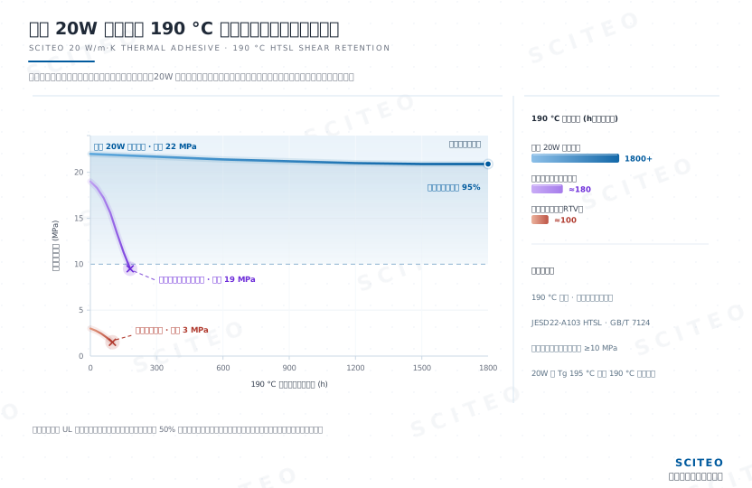
Test-Method Conventions: Why One Formulation Reports Three Numbers
A two- or three-fold spread between datasheet values for the same high-thermal-conductivity adhesive usually reflects a difference in method, not in formulation. Reviewers should require the vendor to state the method, the test pressure and the bond line thickness, then re-measure interfacial resistance under the target conditions. Comparing single figures off two datasheets is like measuring one part with three different rulers.
The four common methods measure physically different quantities.
Steady-state heat flow (ASTM D5470) clamps the sample between temperature-controlled hot and cold plates, establishes a one-dimensional steady heat flux and reads the temperature gradient from a thermocouple array. The direct output is thermal impedance in K·cm²/W or °C·cm²/W. For non-homogeneous materials the standard calls for apparent thermal conductivity rather than intrinsic conductivity, because the measured value already includes the contact resistance of both interfaces and depends strongly on test pressure and bond line thickness. The current edition is ASTM D5470-17(2024), and its scope is limited to electrically insulating materials, so conductive thermal adhesives need a different convention. Its engineering value is that it best represents the assembled state, which also makes it the most conservative.
Laser flash (ASTM E1461) fires an energy pulse at the front face of a thin specimen and records the temperature rise at the back face. The output is thermal diffusivity, converted to conductivity through k = α·ρ·Cp. It characterizes the bulk material only and excludes interfacial contact resistance, so readings run systematically higher than steady-state values. The method is also unsuitable for paste-like and soft compressible materials, which must be consolidated before measurement.
Guarded heat flow meter (ASTM E1530) adds a guard heater around the measurement stack to cut lateral losses, improving accuracy, and typically reports values one step higher again. Transient plane source (ISO 22007-2:2022) and hot wire (GB/T 10297) serve as complements: the former resolves axial and radial conductivity in anisotropic materials, while the latter is limited to materials below 2 W/m·K and is explicitly not intended for arbitration.
One pattern keeps surfacing in our re-measurements: the same formulation can show a several-fold difference in thermal impedance between a 25 μm and a 100 μm bond line. That spread is larger than the conductivity gap between competing formulations. SCITEO therefore ships every dataset with its test method and boundary conditions, and recommends that customers validate on three lines at once: bulk conductivity (E1461), interfacial resistance at target pressure and target bond line thickness (D5470), and device-level junction-to-case resistance (JESD51-14 transient dual interface, with T/CASAS 016-2022 covering the discrete SiC MOSFET flow). A material is only reproducible when all three hold.
Material Solutions for High-Value Heat Flux Interfaces
GaN RF Power Amplifiers and Active Antenna Units
Device-level heat flux has reached the 100 W/cm² class, yet junction temperature stays capped near 150 °C, leaving only tenths of a kelvin per watt of thermal budget at the device-to-heatsink interface. The material must deliver low thermal resistance, low stress and long-term outdoor weathering at the same time.
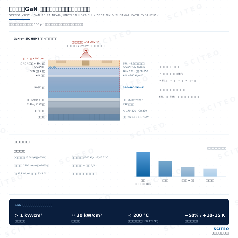
GaN RF devices face two thermal bottlenecks. Inside the device, peak heat flux from a GaN HEMT can exceed 100 W/cm² at the gate fingers, climbing into the kW/cm² range in the hottest spots, and heat must cross the epi-to-substrate interface, where thermal resistance is itself a limiting term. That is why GaN-on-SiC became the mainstream route, with silicon carbide substrates at roughly 400 to 490 W/m·K, close to three times that of silicon. Substrate and carrier design evolves alongside it: aluminum nitride ceramic substrates combine insulation with 170 to 200 W/m·K conduction, copper-molybdenum and copper-tungsten carriers satisfy heat spreading and CTE matching at the same time, and highly integrated T/R modules still attach the power die to the carrier by AuSn eutectic soldering before mounting the carrier to the housing. The frontier is moving further: some designs now embed GaN devices directly in a thin single-crystal diamond layer, using diamond's thermal conductivity to even out the hot spots and buy reliability margin for 6G and satellite links. Outside the device, the assembly interfaces between the power transistor, the heat spreader, the housing and the heatsink are exactly where the materials discussed here are applied.
System-level trends tighten the window further. Massive MIMO has moved from 64T64R toward 128T128R, per-site AAU power reaches 1.2 to 3.5 kW, and microchannel liquid cooling cuts effective thermal resistance to roughly one fifth of an air-cooled design. Once cooling capacity improves, the bottleneck returns to the interface layers inside the package. Outdoor deployment adds humidity, salt fog and wide temperature cycling, so the material must keep the interface intact from −40 to 105 °C and pass 85/85 and salt spray validation.
For this duty, SCITEO custom grades at 40 and 60 W/m·K cover bonding and potting between the power device, the heat spreader and the housing, with CTE available down to 8 ppm/°C, mobile ion content below 5 ppm and shear strength above 30 MPa. Single-component heat-cure systems remove the mixing step, and their batch-to-batch consistency suits narrow-gap dispensing and shape retention inside RF cavities.
Turbo System Power Electronics and Actuator Interfaces
Electronic modules sitting next to the turbine and exhaust side run continuously at 150 to 200 °C and reach 200 to 400 °C where they attach directly to housings. They must survive high temperature, oil swelling, coolant attack and high-frequency vibration at the same time.
Electrification of boosting systems has raised the difficulty of this interface by a full level. Electronic actuators on turbo and electric boosting units, integrated inverters, fuel cell electric compressor controllers and the drive modules of oil-free centrifugal compressors are typically mounted 100 to 300 mm from the exhaust manifold and turbine housing, where metal surface temperatures reach 150 to 200 °C at full load in gasoline applications. The controller body itself runs at 120 to 150 °C, dissipating 5 to 15 W, and component junctions can reach 160 to 180 °C when the thermal path is inadequate. The jump from cold start to full load completes within minutes, and a single climate year accumulates more than 100 thermal cycles.
The reliability requirement set is expanding as well. High-speed motors in electric boosting units exceed 150,000 rpm, fuel cell electric compressors are specified for 25,000 hours of life and more than one million start-stop cycles, and oil-free centrifugal compressors entering data center liquid cooling and commercial HVAC duty are expected to run maintenance-free. Any interfacial delamination shows up first as rising thermal resistance and efficiency loss, then amplifies into a power penalty for the entire boosting or compression unit.
Chemical and mechanical loads arrive together. Engine oil and transmission fluid diffuse into the polymer network, causing hydrocarbon swelling, volume gain and modulus loss. Ethylene glycol coolant at 80 to 105 °C penetrates rapidly from the interface side. Fuel, brake fluid, salt fog and cleaning agents stack on top. On the mechanical side, threaded fasteners relax under sustained vibration, which makes structural bonding the more reliable option, provided the bond line carries sufficient shear strength and elongation.
The material requirements therefore converge on four items: Tg above 200 °C with a post-cure step, where crosslink density and aromatic content set hydrocarbon swelling resistance; CTE in the 12 to 20 ppm/°C range to match aluminum housings and printed circuit boards; shear strength above 30 MPa to resist vibration fatigue; and insulation with low ionic content for long-term safety on the high-voltage drive side. SCITEO supplies a dedicated custom epoxy specification for these interfaces at 10 W/m·K class conductivity with Tg above 200 °C, CTE held within 20 ppm/°C and shear strength above 30 MPa, validated through −55 to 200 °C thermal cycling, engine oil and coolant immersion, salt spray and 85/85 aging, and processed as a single-component heat-cure system that fits existing takt times.
Energy Storage PCS and PV Inverter Power Modules
With 1500 V DC buses, 3 MW-class single units and liquid cooling now standard in utility-scale storage, the module interface carries high-voltage insulation and long-cycle thermal fatigue at the same time.
PCS power ratings are moving fast. Single units have advanced from 2.5 MW to 3.15 and 3.5 MW, centralized designs aimed at 6.25 MWh battery cabins are increasingly common, and power density is up 20% to 40%, while liquid cooling has shifted from option to default. Public product data quantifies the payoff: a dual cooling architecture combining liquid cooling and top-exhaust airflow lowers full-load IGBT temperature by 10 to 16 °C and extends power module life by roughly 25%; integrated cold plates push system thermal resistance below 0.1 K/W; and 2000 V SiC devices on the inverter side cut die junction temperature by a further 5 to 10 °C. As the DC platform rises to 1650 V and 1500 V systems, insulation margin and creepage distance requirements move up with it.
These figures point to one mechanism: the stronger the heatsink or cold plate, the higher the stress the interface layer absorbs. The module base and the cold plate must conduct heat and provide electrical isolation at the same time; outdoor enclosures rated IP65 and C5 corrosion class demand hydrolysis and salt spray resistance; and continuous high-rate charge and discharge cycles drive the interface through repeated shear from −40 to 105 °C. SCITEO addresses this with insulating thermal potting and structural bonding systems from 2 to 11 W/m·K, volume resistivity held at the 10¹⁵ Ω·cm level, shear strength above 30 MPa, CTE in the 20 ppm/°C range, interfacial resistance drift within 5% after 1000 thermal cycles, and shear retention above 90% after long-cycle 85/85 aging.
Data Center Server Power and Servo Drives
Server power has evolved from a single PSU inside the chassis into a rack-level power architecture, with rack power moving from tens of kilowatts toward the megawatt class. The interface material must cover magnetic component hot spots, insulation aging and a decade of uninterrupted service.
Efficiency and space define the generation boundaries. Early Gold and Platinum supplies were rated below 1200 W with end-to-end efficiency under 94%. Titanium-class digital supplies pushed ratings to 1600-3200 W and required at least 96% efficiency at 50% load. The 3200-5500 W generation that followed adopted N+N and N+M redundancy with dynamic current sharing to handle multiphase load surges. Rack-level centralized architectures then abandoned distributed in-chassis supplies in favor of a 50 V DC busbar. The bar keeps rising: 80 PLUS has added a Ruby level, which raises the requirement for redundant supplies to 96.5% efficiency at 50% load with a power factor above 0.96.
Each power-architecture generation pushes more thermal and insulation constraint down to the interface layer. Under the ORv3 specification, a 50 V busbar carries rack power into the 200 to 250 kW range; single-phase power supply units start at 5.5 kW, a shelf built from three-phase 12 kW units delivers 72 kW, and four shelves in parallel reach 288 kW. As racks push past 400 kW, current on a 50 V busbar stops being economical. The industry answer is to move the power components out of the compute rack into an 800 VDC busbar and a dedicated power rack, with power supply, battery backup (BBU) and capacitor bank units carrying megawatt-class load together and cutting copper requirements by nearly half; rack-adjacent 800 VDC sidecars already deliver 400 to 900 kW per unit, which raises bus voltage and creepage distance requirements across the board. On the topology side, interleaved totem-pole PFC, three-level flying-capacitor PFC and three-phase LLC have become mainstream, with SiC and GaN devices operating stably between 100 kHz and 500 kHz. Magnetic components shrink dramatically as a result, at the cost of more concentrated winding and core hot spots: the thermal path of planar transformers and integrated magnetics depends almost entirely on the interface material.
Material requirements shift accordingly. Magnetic components and power devices need thermally conductive insulating potting covering 2 to 20 W/m·K, volume resistivity held at the 10¹⁵ Ω·cm level to support high-voltage busbars and creepage requirements, ionic content below 5 ppm to prevent electrochemical migration under humidity and high-voltage bias, and outgassing plus CTE matched to aluminum housings and printed circuit boards. Servo drives push the requirement one step further: DC bus voltage is moving from 400 V to 800 V, and the interface material must absorb partial discharge stress from high-frequency PWM on top of thermal duty. SCITEO covers this with 2 to 20 W/m·K thermal potting and structural bonding for magnetic components, power devices and busbar fixation, with tunable thixotropy and viscosity for both dispensing and printing.
High-Power LED and UV-LED Modules
LED lifetime is not a device property but a function of junction temperature: every 10 °C the case temperature exceeds the tested point nearly halves the projected life.
Two lighting standards frame the issue. IES LM-80-21 specifies lumen and color maintenance measurement at 55 °C, 85 °C and a manufacturer-selected point, commonly 105 °C, for a minimum of 6000 hours. IES TM-21 projects that measured data to an L70 life. The review focus is not the headline lifetime figure but the gap between the case temperature stated in the report and the case temperature measured in the finished luminaire, because that gap is where the life discount comes from.
The thermal resistance chain is equally explicit. Junction-to-case resistance is set by the packaging process and typically runs 2 to 5 °C/W for COB structures. Case-to-heatsink resistance is set by the interface material, typically 0.1 to 0.5 °C/W. Heatsink-to-ambient resistance is a mechanical design outcome. In a 10 W module the total sits near 6 °C/W, so the interface share looks small, yet it is the segment most likely to degrade over time: once delamination or dry-out starts, its resistance climbs far faster than the other two. Photoelectric conversion efficiency also falls as junction temperature rises, and phosphor and encapsulant degradation shifts color, turning chromaticity drift into a hard acceptance risk for lighting projects.
UV-LED and automotive lamp modules raise the bar again with higher current density, a larger in-package temperature rise and optical cleanliness that is sensitive to outgassing. SCITEO insulating thermal grades for optoelectronic modules cover 2 to 9 W/m·K with low condensable volatiles and yellowing-resistant formulations, compatible with aluminum and ceramic substrate carriers.
Material Boundaries at the Phonon Scale
Production formulations define what can be delivered today; material limits at the phonon scale define how far that curve can still rise.
Hexagonal boron nitride (h-BN) combines electrical insulation with high thermal conductivity. Its in-plane conductivity reaches 300 to 400 W/m·K, and 585 W/m·K in isotopically enriched single crystals, while through-thickness conductivity is only 2 to 10 W/m·K, an anisotropy spanning nearly two orders of magnitude. Add a low dielectric constant and high-temperature chemical stability, and it becomes a natural fit for high-voltage insulating interfaces. That anisotropy is exactly why alignment earns its keep: turning the platelets edge-on so their high-conductivity basal planes point through the bond line is the only way to open a real heat path across it. The bottlenecks sit at both ends. Van der Waals forces between platelets drive agglomeration and demand covalent or non-covalent modification alongside dispersion control; alignment routes such as vertical alignment, ice-templating and 3D-printed skeletons still sit partly in the laboratory. The industry has now pushed through-thickness conductivity into the 5 to 12 W/m·K range in vertically aligned boron nitride skeletons, and bridging the platelets with trace reduced graphene oxide is narrowing the process window further. Dispersion control also sets the loading ceiling, which is why high-loading production formulations still rely on alumina systems. SCITEO's route on this path combines vertically aligned boron nitride networks with covalently modified interfaces to make the through-thickness path real, inserting first at high-value small-area interfaces and moving down the cost curve as the process matures.
Another name shows up more often in the literature: cubic boron arsenide (c-BAs). First-principles calculations put its room-temperature thermal conductivity above 2000 W/m·K; single-crystal experiments landed the figure in the 1300 W/m·K range and isotope-enriched samples reached 1500 W/m·K; nanosecond transducer-less time-domain thermoreflectance has since reported values above 2000 W/m·K, cross-checked on the same samples by conventional TDTR, with a ~1/T² temperature dependence that points to four-phonon scattering and provides rare experimental validation for high-order phonon theory. Its engineering limits are equally explicit: boron melts above 2000 °C while arsenic sublimes heavily from 614 °C, chemical vapor transport growth runs in weeks, temperatures above 920 °C favor a more stable sub-phase, and phonon mean free paths are extremely sensitive to impurities and point defects, leaving no scalable route to large-area single crystals or films. By current process capability, it serves better as a model material that defines the upper bound of phonon transport. It is not the only breakthrough of its kind: a recent Science report describes single-crystalline theta-phase tantalum nitride at roughly 1100 W/m·K at room temperature, nearly three times that of copper, which shows that even the transport ceiling on the metal side is being redrawn.
The value of these systems is not near-term delivery. It is measuring the physical ceiling of the heat path: once a filler skeleton or a single-crystal body can take over transport, the thermal ceiling of the polymer matrix stops being the end point, and for SCITEO it defines the boundary that formulation redundancy has to be sized against.
Selection Quick Reference: High-Thermal-Conductivity Interface Materials
The table below compresses the mechanisms above into an executable checklist for direct comparison during process and R&D review:
| Application | Heat Flux | Dominant Failure | Primary Check Item | SCITEO Direction |
|---|---|---|---|---|
| Turbo system power electronics and actuators | 20-100 W/cm² | Actuator thermal drift, oil swelling | Tg above 200 °C, CTE ≤20 ppm/°C, oil and coolant resistance | Custom epoxy thermal specification, 10 W/m·K class, single-component heat cure |
| GaN RF power amplifiers and AAUs | 100-500 W/cm² | Local hot spots, gain compression | Above 40 W/m·K, CTE below 30 ppm/°C, low outgassing | Structural thermal adhesive, 40/60 W/m·K custom grades |
| Energy storage PCS and PV inverter modules | 50-150 W/cm² | Junction drift, potting cracks | High insulation, hydrolysis resistance, 85/85 and salt spray | Insulating thermal potting and structural bonding, 2-11 W/m·K |
| Data center server power and servo drives | 10-50 W/cm² | Magnetic component hot spots, insulation aging | Volume resistivity ≥10¹⁵ Ω·cm, low outgassing, CTE matching | Thermal potting and structural bonding, 2-20 W/m·K |
| High-power LED and UV-LED modules | 20-100 W/cm² | Accelerated lumen decay, color shift | Rcs 0.1-0.5 °C/W, low CVCM, yellowing resistance | Insulating thermal grades 2-9 W/m·K, low-outgassing formulations |
| High-power die and power module interfaces | above 150 W/cm² | Interfacial fatigue, resistance drift | Interfacial resistance ≤0.05 °C·cm²/W, drift ≤5% after cycling | Structural thermal adhesive 2-60 W/m·K, CTE ≤8 ppm/°C custom grade |
Put the Interface Evidence into the Acceptance Terms
Thermal conductivity is an intrinsic material property. Interfacial thermal resistance is a system property. The distance between them is filled by test convention, bond line thickness, contact quality and service environment, and if any of those remains unquantified, the capability of the material cannot be realized in the finished product.
For high-thermal-conductivity adhesive reviews, SCITEO recommends three fixed steps: confirm the test method and boundary conditions behind the conductivity figure, re-measure interfacial resistance at target pressure and target bond line thickness, and write resistance drift and shear retention after thermal cycling into the acceptance terms. Once those three are complete, the data becomes comparable across suppliers and survives scrutiny during ramp and field service. From turbo system power electronics to energy storage PCS, server power and high-power optoelectronics, heat flux density will keep rising. SCITEO Advanced Materials supports these interfaces with thermal grades from 2 to 60 W/m·K, a reproducible interfacial measurement framework and a frontier filler pipeline that leaves margin in the design.
This article is SCITEO Advanced Materials original technical content; unauthorized reproduction is prohibited.
Appendix: Process & Engineering Adhesive FAQ Index
Why do two suppliers quote different thermal conductivity values for the same high-thermal-conductivity adhesive?
Most often the methods differ, not the formulation. Steady-state heat flow (ASTM D5470) includes the contact resistance of both interfaces and reports thermal impedance together with apparent conductivity, which reads conservatively. Laser flash (ASTM E1461) measures bulk thermal diffusivity and converts it with density and specific heat, so it reads systematically higher. A guarded heat flow meter (ASTM E1530) usually reads higher again. Ask the vendor to state the method, the test pressure and the bond line thickness, then re-measure interfacial resistance under actual operating conditions. SCITEO ships both the bulk value and the interfacial value.
Thermal conductivity meets spec but the system still exceeds its junction temperature target. Where should we look?
Usually at the interface, not the bulk material. Three common causes: bond line thickness runs thick and resistance scales linearly with thickness, because dispense volume, compression pressure and die flatness all drift; voids or incomplete wetting reduce true contact area and concentrate heat flux into the remaining area; and service-time slip or delamination pushes resistance up non-linearly. Start with a transient junction-to-case measurement to locate which interface dominates, then confirm void content and thickness with scanning acoustic microscopy and cross-sectioning before returning to formulation.
Grease and gap pads have worked fine. When does the design have to move to a curable thermal adhesive?
When the duty cycle demands high temperature, a thin bond line and structural fixation at the same time. Thermal grease has no bond strength: its carrier oil bleeds and oxidizes under sustained heat, and the interface takes repeated shear migration through thermal cycling, degrading through pump-out, dry-out and squeeze-out, so resistance multiplies over service life. A gap pad holds contact through assembly pressure and compression rebound, but rebound fades after long exposure to heat and it is floored by a minimum thickness, so a micron-scale bond line cannot be pressed down. Only a curable structural thermal adhesive locks bond line thickness, CTE and bond strength together. Conversely, where the interface is reworkable, pressure is ample and temperature swings are mild, grease remains the lower-cost, sensible choice.
For thermal potting in energy storage PCS and PV inverters, why do ionic content and hydrolysis stability matter together?
Because these units run under combined humidity, salt fog and high-voltage bias for years. Free chloride and sodium ions migrate electrochemically under field and moisture, and insulation resistance can drop by orders of magnitude within a few hundred hours. If the matrix lacks hydrolysis resistance, interfacial debonding and leakage current appear at the same time. The engineering gate is long-cycle 85/85 aging with both insulation and shear strength holding, ionic content within 5 ppm, and salt spray validation on top, which matches the IP65 and C5 requirements of outdoor cabinets.
How do thermal insulation potting requirements for data center server power differ from a conventional power supply?
The difference sits in duty intensity and insulation level. Rack-level architectures concentrate supplies onto a 50 V DC busbar: single-phase units start at 5.5 kW, and a shelf built from three-phase 12 kW units delivers 72 kW. Once rack power exceeds 250 kW the busbar current stops being economical, so the power components move out of the compute rack into an 800 VDC busbar and a dedicated power rack, which raises bus voltage and creepage distance requirements. The potting material must cover 2 to 20 W/m·K, hold volume resistivity at the 10¹⁵ Ω·cm level, keep ionic content within 5 ppm, and pass long-term heat aging and 85/85 validation for more than a decade of service without opening the cabinet.
What does hexagonal boron nitride contribute to insulating high-conductivity interfaces, and why has it not yet replaced alumina at scale?
Its value lies in combining electrical insulation with high thermal conductivity. In-plane conductivity reaches 300 to 400 W/m·K while through-thickness conductivity is only 2 to 10 W/m·K, and it pairs low dielectric constant with high-temperature chemical stability, which suits high-voltage insulating interfaces. The bottlenecks are twofold: van der Waals forces between platelets cause agglomeration and require covalent or non-covalent modification plus dispersion control, and alignment processes are hard to scale, so vertical alignment, template pore-forming and 3D-printed skeletons remain mostly laboratory routes. SCITEO expects insertion to start at high-value small-area interfaces and move down as the process matures.
How thin should the bond line be for a thermal adhesive, and is thinner always better?
Thin is the right direction, but thickness cannot be optimized on its own, apart from pressure, rheology and surface flatness. Interfacial resistance is the sum of a bulk term (thickness divided by conductivity) and a contact term; halving the thickness halves the bulk term, yet once the layer is compressed to the scale of filler particle size and surface roughness, the contact term takes over and can even worsen the result through incomplete wetting and voids. In practice, 25 μm is the convergence target for a high-thermal-conductivity structural adhesive, and the measured interfacial resistance at target pressure, not the thickness number alone, is the figure to qualify against.