Semiconductor-Grade Die-Attach Conductive Silver Adhesive: Adhesion, Volume Resistivity and Thermal Conduction Trade-Offs, Plus Resin Bleed-Out, Void and Silver-Migration Control
SCITEO conductive silver and sintered silver platforms: from silver flake grading and percolation thresholds to volume production across chip packaging, printing and automotive power modules
Abstract
Solder paste has been showing its limits more clearly every year. Once pitch drops below 0.65 mm, printing starts to bridge and void rates get hard to hold; parts that cannot tolerate reflow above 230 °C, such as MEMS, film capacitors and already-populated modules, cannot go through a reflow oven at all. Electrically Conductive Adhesive (ECA) fills that gap with lead-free chemistry, a low process temperature and enough mechanical strength, which is why it is now routine for die attach, precision crystal oscillators, MEMS sensors and power-module interconnect.
Selection logic, though, is not a single-metric exercise. Lower volume resistivity is not automatically better, and the datasheet will never say so: adhesion, volume resistivity, thermal conductivity and ionic purity trade against one another, and pushing any single metric to its limit typically shows up during power cycling, biased humidity or high-temperature aging rather than on the bench.
How those four parameters constrain each other is the first order of business. The article then returns to the dispensing and curing line to work through the causes and countermeasures behind three volume-production defects (resin bleed-out, interfacial voids and silver migration), and closes with a selection table to check against. Data comes from SCITEO's conductive silver and sintered silver systems and their volume-production validation at semiconductor packaging customers.
Core Parameter Comparison
Putting the three systems side by side makes the differences easier to read:
| Parameter | SCITEO Solution | Industry Typical | Test Standard |
|---|---|---|---|
| Volume resistivity (epoxy silver) | 3×10⁻⁵ Ω·cm | 10⁻⁴ Ω·cm class | ASTM D257 |
| Volume resistivity (sintered silver) | 2×10⁻⁶ Ω·cm | Not applicable | Four-point probe |
| Thermal conductivity (epoxy silver) | 5–60 W/m·K | 1–5 W/m·K | ASTM D5470 |
| Thermal conductivity (sintered silver) | 280 W/m·K | Not applicable | ASTM D5470 |
| Tg | 140–195 °C | 80–120 °C | DMA / DSC |
| CTE | <30 ppm/°C | 50–80 ppm/°C | TMA |
| Initial shear strength | 19 MPa | 5–10 MPa | GB/T 7124 |
| Cure linear shrinkage | <0.3% | 1–3% | ISO 2577 |
| Mobile ions (Cl⁻/Na⁺/K⁺) | <10 ppm | above 50 ppm | IC ion chromatography |
| Low-temperature cure | 60–80 °C | 120–160 °C | DSC |
The SCITEO conductive silver portfolio currently covers four stable directions:
- Heat-cure silver: 19 MPa initial shear strength (GB/T 7124), Tg 140–195 °C, and CTE <30 ppm/°C, matched to high-UPH production cadence.
- Low-temperature silver: 60–80 °C cure, compatible with film capacitors, flexible substrates, and MEMS.
- High-conductivity silver: 5–60 W/m·K (ASTM D5470) for LED optoelectronics, automotive electronics, and power devices.
- Sintered silver: 2×10⁻⁶ Ω·cm volume resistivity and up to 280 W/m·K thermal conductivity (pressure-assisted sintering, ASTM D5470), at the upper end of what the material delivers in volume.
I. Where SCITEO Conductive Silver Earns Its Place
Soldering heat damages heat-sensitive parts, and lead-bearing alloys fail environmental rules; those two constraints have pushed a lot of processes toward conductive silver. Process adaptability matters, but the deeper reason it still has no substitute across the precision domains below is that its electrical and mechanical performance can hold at the same time instead of one buying the other.
Semiconductor Chip Packaging (Die Attach)
Die attach fixes the bare die to a leadframe, QFN, or BGA substrate. Because the die backside usually carries a silver or gold finish, the bond line serves three functions at once: mechanical fixation, ohmic contact, and backside heat removal. Wafer-level die attach moves the same step ahead of singulation and tightens the bar further on bond-line consistency, void-free fill, and low cure shrinkage. For wide-bandgap power devices (SiC, GaN), backside thermal conduction sets the junction-temperature ceiling and the power-cycling lifetime directly.
Take SiC power-module die attach. Junction temperature clears 175 °C without strain, and the roughly 4.2 ppm/°C-to-17 ppm/°C CTE mismatch between SiC and a copper substrate turns every power cycle into reciprocating shear inside the bond line; conventional ECA develops interfacial micro-cracks and climbing thermal resistance within a few hundred cycles. That stress cannot be designed away. The workable route is to spread it across the whole interface rather than concentrate it at isolated micro-bumps, which is exactly what SCITEO builds into a single heat-cure system, high Tg (140–195 °C), low CTE (<30 ppm/°C) and low cure shrinkage together, so the bond line holds both adhesion and thermal stability through module-level power cycling (PCsec) and temperature cycling, leaving verifiable interfacial headroom for automotive and industrial power modules.
Advanced packaging as a whole is migrating toward heterogeneous integration. CoWoS-L carries multiple compute chiplets on local silicon bridges, and panel-level packaging (CoPoS) trades round wafers for square glass or organic carriers to gain usable area. Hybrid bonding's rollout is also being recalibrated: after JEDEC raised the HBM4 stack-height ceiling to 775 μm, 16-Hi HBM4 still relies on micro-bumps with molded underfill (MR-MUF), while copper-to-copper hybrid bonding slips to HBM4E and possibly HBM5; the acceleration is on the logic-chiplet side, where SoIC-class bond pitch has moved from 9 μm to 6 μm and is heading for 4.5 μm. Either way, die-attach interconnect is being pushed toward finer pitch and lower thermal resistance: bond line thickness (BLT) has to compress below 25 μm while still filling large-die areas without voids. Filler grading and rheology are the levers iterated against exactly that constraint.
Precision Crystal Oscillators
The hard part in crystal oscillators is that the quartz blank is itself a stress-sensitive element. Resonant frequency is set by blank geometry and preload together, and the die-attach layer writes into that preload through cure shrinkage, modulus and thermal expansion: quartz and a ceramic base differ by 3-5 ppm/°C in CTE, so shear stress from temperature cycling drifts the equivalent series resistance (ESR) and quality factor (Q), and the frequency-temperature characteristic (TCF) walks off its factory calibration. Customer process issues concentrate on the same chain. An oversized or off-center dispense dot loads the blank asymmetrically and shows up as frequency scatter within a lot; too fast a ramp locks stress in during shrinkage and pushes the aging rate (ppm/year) up; adhesive creeping up the blank edge shifts the effective mass, moving frequency directly and, in bad cases, degrading the electrode contact. Holding interface stress and cure displacement down is a delivery item on this interface, right alongside the conductive path.
SCITEO grades for this interface deliver 18 MPa room-temperature die shear (MIL-STD-883 Method 2019) while leaving enough dispense and cure-displacement margin around the blank; with mechanical retention and interface stress both under control, long-term aging stability holds.
Sensors and Automotive Electronics
Engine-compartment temperatures span −40 °C to 150 °C and beyond. What a wide temperature domain demands is a stable storage modulus and low-stress behavior at both ends, or the interface delaminates as internal stress accumulates under thermal shock. A SCITEO grade at 195 °C Tg covers continuous operation at the hot end; cryogenic grades hold at −70 °C. Pressure, acceleration and current sensors also care about drift, where low-stress, low-absorption formulations visibly limit zero-point shift. The same sensor often has to clear AEC-Q temperature cycling and biased damp heat together, and wide-temperature and moisture resistance cannot be solved as two separate problems.
Printing and High-Volume Assembly
In SMT high-volume placement and thick-film screen printing, pot life and cure window set line takt and scheduling flexibility. Printable conductive silver delivers more than 48 hours of room-temperature working life, so printing, placement and cure can be scheduled without breaking cadence; one part number spans a 60–150 °C cure window across different substrate thermal masses and oven types. Whether the line wants a low-temperature slow cure to protect heat-sensitive substrates or a high-temperature fast cure to lift UPH, the choice follows actual line conditions, with no need to keep swapping part numbers to fit a process window. Line-change loss and window mismatch usually cost more than the material price difference.
AI Compute and Photonic Interconnect
Once single-die thermal design power passes 500 W, package-level hotspot heat flux goes beyond 1000 W/cm², and electrical and thermal conduction stop being separable objectives: one filler skeleton has to deliver both. The power side is moving faster. The 800 V high-voltage DC (HVDC) architecture that NVIDIA, Google and Microsoft are driving through OCP is already scheduling MGX-compatible 800 VDC power racks, with megawatt-class Kyber racks following; a simpler distribution chain actually squeezes the electrical-insulation and thermal-stability margin left to the interface material. The optical side is tightening too: co-packaged optics (CPO) puts the switch die and the optical engines in one package, where switch ASIC junction temperature can reach 105 °C while InP lasers typically top out at 70–85 °C. External laser source (ELS) designs have therefore become the mainstream answer, and the laser die inside a COS/COC or ELSFP module still relies on the die-attach layer to carry heat out. Such interfaces need low volume resistivity, high thermal conductivity and low outgassing to hold simultaneously, and ideally out of one filler skeleton rather than stacked layers; that is why SCITEO's high-conductivity silver and sintered silver lines share a single powder-grading logic, so signal integrity and junction temperature still have margin under high-frequency switching.
Flexible Sensors and Robotic Tactile Sensing
Flexible capacitive pressure sensors move the electrodes off rigid boards and onto PI, PET or PDMS films, where screen-printed interdigital silver electrodes form a capacitor array that conforms to curved surfaces. Robotic dexterous hands take the same route and are moving faster: current whole-hand tactile solutions split the work across fingertip, finger pad and palm, with tactile points on a single fingertip now in the thousands, resultant-force resolution in the 30 mN range, electronic-skin force resolution in the 10 mN range, and contact-life targets at a million cycles. What these electrodes need is close to the opposite of die attach. Resistance has to stay stable after many thousands of bend cycles, because any shift in electrode resistance rewrites the RC time constant and contaminates the capacitance readout; under fast dynamic sampling, the weak differential signal is buried first. Flexible substrates also leave very little thermal budget, so cure temperature has to stay below the substrate limit, while the electrode-to-PDMS or electrode-to-silicone interface must survive repeated deformation without delaminating or outgassing. For a tactile sensor, the accuracy ceiling ends up being the electromechanical consistency of the electrode.
II. The Underlying Logic of Four Core Parameters
Every figure on a datasheet maps to a defined physical or chemical mechanism. Only by putting it back into a failure scenario does the trade-off become a decision.
Adhesion: Interfacial Shear Strength and Thermomechanical Stress Balancing
A bond line that peels off easily after cure usually gets written off as bad adhesive. The more accurate reading is that weak adhesion shows up in two ways, material delamination and silver flakes debonding from the resin matrix, and the fracture location tells them apart. Interfacial failure sends you to surface preparation and wetting; cohesive failure sends you back to formulation and degree of cure.
The dominant failure driver in chip packaging is CTE mismatch. Silicon die (~2.6 ppm/°C) and copper leadframe (~17 ppm/°C) differ sharply, so thermal cycling imposes reciprocating shear inside the adhesive layer. If Tg and modulus are poorly engineered, that stress has nowhere to go: micro-cracks initiate at the interface, followed by bond failure and an abrupt resistance rise. Large die are harder. Stress forms a gradient through the bond line, and shear concentration at the edges runs markedly higher than at the center.
The heat-cure approach pairs high Tg (140–195 °C) with low CTE (<30 ppm/°C), then uses filler grading to pull cure linear shrinkage below 0.3% (ISO 2577). Low shrinkage means low residual tensile stress at the interface; sufficient modulus means shear spreads across the bond line instead of concentrating at isolated micro-bumps. SCITEO's grades in this class deliver 19 MPa initial shear strength (GB/T 7124) while clearing JEDEC MSL (moisture sensitivity level) and TCoB (board-level thermal cycling), and the fracture path stays consistent before and after aging.
Volume Resistivity: Percolation Threshold and the Silver-Loading Trade-Off
"Lower resistance" is the request engineering and procurement raise most often. The request is fine; treating it as the only direction to optimize is not.
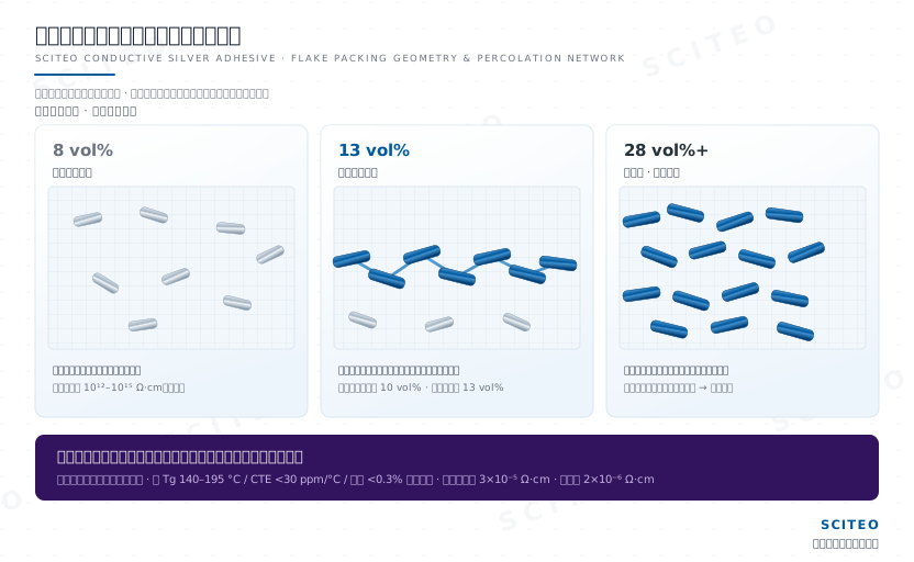
Conduction in a conductive adhesive follows percolation theory. Once the silver filler's volume fraction passes the critical threshold, flakes interconnect into a continuous conductive network characterized by ρ = R·A/L. Micron-scale flakes (conventional ECA) conduct through physical contact, typically at the 10⁻⁴ Ω·cm level; SCITEO conductive silver reaches 3×10⁻⁵ Ω·cm (ASTM D257).
The cost sits downstream. Raising silver loading to chase lower resistivity starves the resin fraction and takes adhesion and dispensing processability down with it, because past the threshold the percolation curve enters diminishing returns quickly, a sentence no datasheet prints. Nano sintered silver takes a different route: silver nanoparticles fuse metallurgically at relatively low temperature through surface energy, eliminating interfacial contact resistance, with volume resistivity reaching the 2×10⁻⁶ Ω·cm class (four-point probe) for high-frequency, high-current interconnect. Further out, silver-coated copper (Cu@Ag) powder splits the difference on cost and electromigration resistance, while sintered copper drops silver altogether and moves the cost into sintering-atmosphere oxidation control. Silver's electrochemical activity remains the constraint this route cannot escape, which is why sintered silver still needs dedicated anti-migration design under biased humidity.
Thermal Conductivity: Phonon Scattering and Filler Grading
Polymers are poor thermal conductors: heat travels mainly as phonons generated by lattice vibration. Those phonons scatter hard at silver-particle/resin interfaces and create significant interfacial thermal resistance, so the real work in thermal modification is making the phonon path one continuous chain rather than simply loading more silver. SCITEO's thermal line therefore runs in two tiers: 5–10 W/m·K high-fill modified silver (ASTM D5470) for conventional LED optoelectronics and automotive electronics, and 20–60 W/m·K high-conductivity silver for wide-bandgap and other high-dissipation duty, where a continuous pure-silver skeleton opens the heat path. Sintered silver reaches up to 280 W/m·K under pressure-assisted sintering (ASTM D5470), at the upper end of what the material delivers in volume. Filler grading, particle-size distribution and interfacial coupling together set how continuous that chain stays, and they are the same three things that move thermal performance from a lab number to a repeatable production value.
Ionic Impurities: Electrochemical Migration and CAF Growth Control
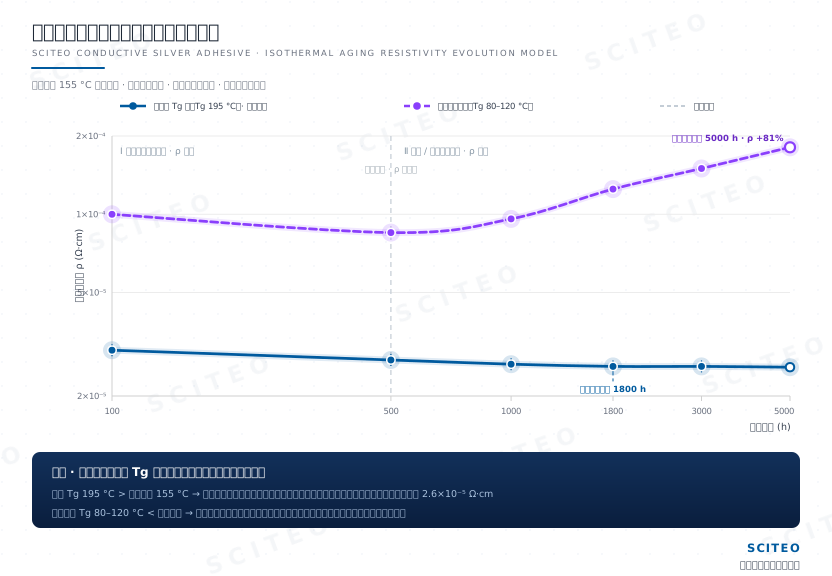
When shorts or corrosion appear after temperature-humidity bias testing (THB/HAST), the root cause usually traces back to ionic impurities. Free chloride (Cl⁻), sodium (Na⁺) and potassium (K⁺) ions in the adhesive migrate electrochemically (ECM) under the combined action of electric field and moisture, dissolving silver at the anode and plating dendrites at the cathode; in severe cases this nucleates conductive anodic filament (CAF) growth along the glass-fiber interface. Low ionic content is therefore not an anti-delamination add-on: it decides whether a nanoscale-linewidth substrate corrodes irreversibly. The industry norm is to hold mobile ions below 10 ppm by IC ion chromatography and to qualify insulation resistance and dendrite growth under bias at 85 °C/85% RH per IPC-TM-650 Method 2.6.14. SCITEO works both ends, with electronic-grade purified resin and surface-passivated silver powder at the raw-material end, and a low-absorption resin backbone that closes the moisture pathway into the bond line.
III. Critical Defects in Advanced Packaging Processes
Conductive silver is demanding on both formulation and production line. Three defect classes carry the most risk in volume production, and they share a signature: an anomaly at a single dispense site or cure lot scales into a batch-level yield loss.
Resin Bleed-Out and Wire-Bond Failure
After die attach, the epoxy fraction creeps onto the gold-plated area around the die pads under capillary action or surface tension. That resin is insulating, so subsequent wire bonding produces non-stick on pad (NSOP) or markedly lower bond pull strength; copper wire is even more sensitive to pad cleanliness than gold, with a narrower tolerance window.
On the material side the levers are the resin system's surface tension and filler wettability, which hold resin bleed-out (RBO) down; on the process side there are substrate plasma-cleaning parameters and dispense volume. Bleed-out also tracks thixotropic structure: a formulation with low yield stress and slow viscosity recovery once shear is removed spreads before cure, and the bleed boundary moves outward with it. In volume troubleshooting, verify substrate cleaning and the cure profile first, then go back to the adhesive formulation; that sequence usually reaches root cause by the shortest path.
Interfacial Voids and Incomplete Cure
Extensive voids under the die on X-ray and an adhesive that stays liquid after heating frequently show up together, because they trace back to the same path.
Voids are not just localized hot spots. Their thermal conductivity is close to zero, so heat flux is squeezed onto the remaining contact area and local current density and junction temperature rise together; the void edge is also a stress concentrator, and cracks usually start there. Beyond trapped air from a closed dispense path, the main causes are moisture condensed during warm-up and low-molecular-weight volatiles inside the adhesive. Vacuum aluminum packaging with cold-chain storage solves only half of that; the other half is a hard requirement for natural room-temperature warm-up, with forced heating prohibited. Condensation from a sharp thermal differential not only leaves voids, it degrades the curing-agent system and shows up as a cure anomaly, and batches accelerated with an oven or hot water almost invariably fail X-ray re-inspection. Void acceptance is tiered by application: consumer and general industrial packaging typically allows up to 10% void area fraction, high-reliability and automotive modules tighten to 5%, and high-power and military criteria push to 2%, judged by scanning acoustic microscopy (C-SAM) together with X-ray. Large die additionally need the dispense path matched to vacuum-assisted cure parameters before void rate comes down.
Silver Migration and Dendritic Shorts
Under high humidity and a DC field, silver ions dissolve from the anode and deposit at the cathode, growing dendritic crystals until the circuit shorts.
Silver is electrochemically active, particularly under biased, humid conditions, and fine-pitch routing has very little tolerance for it: on a silver surface with 0.3 mm spacing, recognizable dendrites can grow within tens of hours at 85 °C/85% RH and tens of volts of bias. Material-side suppression has three layers: silver-particle passivation or encapsulation, dedicated anti-migration inhibitors, and a low-absorption resin backbone. SCITEO applies the first two together in select high-reliability grades to lift THB/HAST performance, suppressing dendrite growth at the material level and lowering electrochemical migration risk on fine-pitch routing.
IV. The Next Leg of Conductive Interconnect
The conductive silver category is being redefined by several larger trends. None of them necessarily becomes a purchase order tomorrow, but each one rewrites where a material platform should put its design weight.
Sintered silver and sintered copper are becoming the mainstream route for power-semiconductor interconnect. SiC and GaN devices push junction temperature past 175 °C, and conventional high-lead solder is reaching its limit on both the environmental and thermal fronts. Nano sintered silver completes metallurgical interconnection at 200–250 °C without applied pressure, landing in the 200 W/m·K class; pressure-assisted sintering pushes that to 280 W/m·K (ASTM D5470), already a mainstream candidate for automotive power-module die attach. The copper side has moved further: oxidation-resistant formulations and ultrafine copper powder brought pressure down from the tens of MPa of early generations to 10–15 MPa and temperature to 200–250 °C. Copper costs far less than silver and is intrinsically free of silver electromigration, at the price of sintering in a reducing or inert atmosphere and holding oxidation under control end to end. SiC module die attach is therefore moving toward parallel silver and copper evaluation, which raises the bar on ionic purity and interfacial densification.
Interface heat flux has changed order of magnitude as well. TDP on high-end compute chips has passed 500 W, localized hotspot heat flux exceeds 1000 W/cm², and every thermal interface inside the package is compressed to its limit, so electrical and thermal conduction have to come from one filler skeleton. The power architecture is rising in step: 800 V HVDC and direct-to-chip liquid cooling have entered rack-level deployment, and the interface material has to hold electrical insulation and thermal stability at both a higher voltage platform and a higher coolant return temperature, two requirements that rarely landed on the same material layer before.
The other end of the temperature domain imposes its own terms. Superconducting quantum chips run in the millikelvin range of a dilution refrigerator, so interconnects must survive repeated cooldowns to liquid-helium temperature without embrittling or delaminating, and keep outgassing low enough not to contaminate the optical and superconducting devices inside a high-vacuum cavity, a far harsher constraint on resin-backbone low-temperature compliance and low-molecular residue than room-temperature service. The same low-temperature, low-stress formulation logic extends downward into cryogenic interconnect, while systems rated above 500 °C take over upward.
What these directions share is that a material platform has to build both ends of the temperature range, the atmosphere and the cleanliness constraints into formulation headroom at project kickoff. Reformulating once a requirement is explicit usually means missing the customer's qualification window. SCITEO front-loads margin at both temperature extremes and in the interface process precisely so that new requirements land inside an existing formulation family instead of starting from zero.
V. Die-Attach Conductive Silver Selection Reference
| Application | Key Failure Mode | Primary Criterion | SCITEO Product Direction |
|---|---|---|---|
| SiC/GaN power-module die attach | Interfacial shear fatigue under power cycling | High Tg, low CTE, module-level PCsec pass | High-Tg conductive silver, nano sintered silver |
| Precision crystal oscillators | Die-attach stress driving frequency drift and ESR degradation | Low cure shrinkage, low stress, 18 MPa die shear | Low-stress conductive silver |
| Automotive electronics and sensors | Wide-temperature interfacial delamination | Stable modulus from −40 to 150 °C | High-temperature and cryogenic conductive silver |
| Heat-sensitive parts and flexible substrates | Cure-induced thermal damage | 60–80 °C low-temperature cure | Low-temperature-cure conductive silver |
| Flexible tactile and pressure-sensor electrodes | Bend-induced electrode resistance drift corrupting the capacitance readout | Low cure temperature, interfacial adhesion, stable resistance after bending | Low-temperature-cure conductive silver, flexible-substrate silver paste |
| Wafer-level and quantum-chip interconnect | Cryogenic contraction stress, low-temperature embrittlement and outgassing | Low-temperature cure, low outgassing, low stress | Low-temperature-cure silver, low-outgassing silver |
| Thick-film printing and high-volume placement | Line-change loss and process-window mismatch | Over 48 h working life, wide cure window | Printable conductive silver |
| High-power and laser die attach | Junction-temperature overshoot, hot spots | 20–60 W/m·K high thermal conductivity | High-conductivity silver, sintered silver |
| AI compute and optical-module interconnect | High heat flux, interfacial thermal resistance | Low volume resistivity, high conductivity, low outgassing | High-conductivity silver, sintered silver |
VI. Conclusion
Conductive silver performance is set by the polymer matrix, rheology control, and powder metallurgy together; it is not glue plus silver powder. From chip die attach to flexible tactile electrodes, every bond shapes the full-lifecycle reliability of the end product. Drawing on long-term application data from semiconductor packaging customers, SCITEO offers a complete series from room-temperature air-drying to ultra-high temperature (above 500 °C), and from low-temperature cure to high-conductivity, ultra-low-resistivity sintered silver. What it delivers is not only material, but full-chain process support from dispensing and curing through reliability validation.
This article is SCITEO Advanced Materials original technical content; unauthorized reproduction is prohibited.
Appendix: Process & Engineering Adhesive FAQ Index
What are the core advantages of SCITEO heat-cure conductive silver over two-component room-temperature systems?
Cure cycle and process window. A heat-cure system finishes in tens of minutes and carries 19 MPa initial shear strength (GB/T 7124), Tg 140–195 °C, and CTE <30 ppm/°C, so it can be matched precisely to component temperature tolerance and to a high-UPH cadence. Two-component room-temperature systems typically need over 24 hours to dry, show wider batch-to-batch volume-resistivity variation, and are harder to tighten on CTE matching and ionic-impurity control, which is where batch consistency most often breaks down.
Does SCITEO offer a low-temperature fast-cure conductive solution for heat-sensitive components?
Yes. SCITEO has developed 60–80 °C low-temperature-cure conductive silver for heat-sensitive assemblies, achieving conductive matching and mechanical bonding without damaging delicate components such as film capacitors and flexible substrates. For high-volume placement, a matched printable conductive silver is also available, balancing low per-unit material cost with stable dispensing consistency.
Can conductive silver adhesive be used immediately after removal from freezer storage?
No. This is the most common process violation behind cure anomalies and interfacial voids. Refrigerated silver adhesive must warm naturally to room temperature (typically 2–4 hours, depending on package size). Never force warming with an oven or hot water, because a sharp temperature differential causes atmospheric moisture to condense into the adhesive, disrupting the cure network and conductive pathways; X-ray re-inspection usually then shows voids under the die.
Resin bleed-out around the pads after die attach is causing gold-wire non-stick. Is this a material problem or a process problem?
Both, but troubleshoot process first and formulation second. Incomplete substrate plasma cleaning, excess dispense volume and long dwell before cure all push the bleed boundary outward; confirm those three before going back to the adhesive. On the material side the levers are the resin system's surface tension, filler wettability and thixotropic structure: a formulation with low yield stress and slow viscosity recovery after shear spreads before cure and is harder to contain. Once bleed-out covers the gold-plated pads, wire bonding yields non-stick on pad (NSOP) or reduced bond pull strength, and copper wire has a narrower tolerance window than gold.
What acceptance criterion applies to die-attach void rate?
Tier it by application, then read it with non-destructive inspection. Consumer and general industrial packaging typically allows up to 10% void area fraction, high-reliability and automotive modules tighten to 5%, and high-power and military criteria push to 2%, judged by scanning acoustic microscopy (C-SAM) together with X-ray, since visual inspection cannot find sub-surface voids. A void conducts almost no heat, so flux is squeezed onto the remaining contact area and local current density and junction temperature rise together, while the void edge becomes a crack initiation site. Large die therefore need the dispense path and vacuum-assisted cure parameters matched to the void-rate target rather than tuned independently.
Why can't a flexible capacitive pressure sensor use a standard die-attach silver adhesive as its electrode?
The constraints are close to opposite. Die attach wants low resistivity and high modulus; a flexible sensor electrode has to hold its resistance steady through repeated bending. Once electrode resistance drifts with deformation, it rewrites the RC time constant and contaminates the capacitance readout, and under dynamic sampling the weak differential signal is the first thing to be buried. Flexible substrates also carry a low thermal budget, so cure temperature must stay below the substrate limit, and the electrode needs enough adhesion to PDMS or silicone to avoid delamination and outgassing under repeated deformation.
Why does SiC power-module die attach have to track CTE mismatch and power-cycling lifetime?
SiC junction temperature can exceed 175 °C, and the roughly 4.2 ppm/°C-to-17 ppm/°C CTE mismatch between SiC and a copper substrate turns every power cycle into reciprocating shear inside the die-attach layer. If that stress cannot be absorbed, micro-cracks initiate at the interface and thermal resistance climbs. SCITEO's high-Tg, low-CTE silver systems homogenize the shear through modulus and filler-grading design, and are validated through JEDEC temperature cycling (TC) and module-level power cycling for long-term automotive power-module reliability.
How does conductive silver adhesive control silver migration and electrochemical migration risk?
Under high humidity and DC bias, silver is electrochemically active: silver ions dissolve from the anode and deposit at the cathode, growing dendrites until the circuit shorts. Suppression works on three layers: silver-particle passivation or encapsulation, dedicated anti-migration inhibitors, and a low-absorption resin backbone. SCITEO combines the first two in select high-reliability grades and works the resin backbone and ionic purity together to cut moisture ingress and free-ion concentration. That markedly improves THB/HAST performance and suppresses dendrite growth at the material level, lowering electrochemical migration risk on fine-pitch routing.