SMT Cold Solder Joints, Solder Voids and Head-in-Pillow: 008004 and SiP Vacuum Reflow
From paste rheology, stencil area ratio and placement downforce to dynamic warpage, sub-2% void rates and 3D AXI tomography: SCITEO's engineering map of SMT defect mechanics and process windows, written for packaging engineers
Abstract
5G, HPC and high-end smart terminals have pushed per-board functional density into a new regime, and surface mount technology has become a composite discipline: non-Newtonian fluid mechanics, micron-scale motion control, heat transfer and optical metrology, all in play at once. Once passives drop to 008004 (0.25 mm x 0.125 mm) and actives arrive as 0.3 mm-pitch BGAs, CSPs and SiP heterogeneous modules packed side by side, tuning parameters by feel stops converging yield.
The defects that are hardest to kill almost all sit at the boundaries between printing, placement and reflow: how paste releases from an aperture only tens of microns wide, the dynamic Z-axis load at the instant a micro-component touches down, and the dynamic warpage that CTE mismatch amplifies during ramp. The solder itself is rarely the culprit.
SCITEO Advanced Materials brings its field experience with electronic packaging adhesives to bear on each physical quantity along that chain: stencil area ratio and transfer efficiency, placement downforce and component micro-cracking, Head-in-Pillow and dynamic warpage, void suppression under vacuum reflow, and the inspection loop built from 3D SPI, 3D AOI and 3D AXI. The rheology and thermo-mechanical values of high-temperature bonding, thermally conductive, sealing and conformal-coating grades go onto the same process window as the equipment parameters.
Bottom line first: the next increment of SMT yield most likely comes from managing interface-material physics and inspection data inside one process window. The margin left in a single machine is close to spent.
Core Parameter Comparison
The table below sets the key process targets for 008004 and SiP assembly beside common industry practice, for line-by-line review:
| Parameter | SCITEO Engineering Criteria | Industry Typical | Test Standard |
|---|---|---|---|
| Minimum component size | 008004 (0.25×0.125 mm) | 0402/0201 | IPC J-STD-001 |
| Micro-component stencil area ratio | ≥0.75 (step stencil + electroform) | near the 0.66 floor | IPC-7525 |
| Stencil aperture transfer efficiency | ≥95% | 70-80% | IPC-7525 |
| 008004 placement downforce | 0.5-1.0 N | Above 2 N | IPC-9701 |
| Dynamic warpage control | ≤0.05 mm/inch | 0.1-0.15 mm/inch | Shadow Moiré |
| Vacuum reflow void rate | <2% | 10-20% | IPC-7095 |
| Vacuum pressure | ≤10 mbar | Atmospheric | Equipment process window |
| Underfill Tg / CTE | ≥150 °C / ≤20 ppm/°C | 100-120 °C / 50-80 ppm/°C | DMA / TMA |
| Mobile ion content | ≤10 ppm (Na⁺/Cl⁻) | 30-100 ppm | IC ion chromatography |
| Multiple 260 °C reflow passes | ≥3 passes, crack-free, hermeticity retained | Cracking on the first pass | J-STD-020 |
| Inspection | 3D SPI/AOI/AXI with AI loop | 2D vision and manual review | IPC-A-610 |
Paste Printing: Shear-Rate Window and Stencil Area Ratio
More than 60% of soldering defects trace back to the printer: shorts, insufficient paste, bridging, tombstoning. Nearly all of them leave a mark in the geometry of the deposit first. This looks like the least technical step on the line. It is a controlled rheology process, and its window is set by three things: paste thixotropy, squeegee kinematics, and aperture geometry. Get any one of them wrong and the deposit turns into a defect at reflow.
Thixotropic Recovery and the Shear-Rate Window
Solder paste is a highly thixotropic non-Newtonian fluid made from alloy powder and flux. At rest, an internal gel network holds apparent viscosity high and the paste sits still on the stencil. The squeegee comes through, shear stress breaks the network apart, apparent viscosity falls by orders of magnitude, and the paste liquefies into the apertures under pressure and gravity. Once the blade passes and shear disappears, viscosity has to climb back within a few hundred milliseconds, or the deposit slumps.
Three failure modes map onto this window. Too much shear separates flux from alloy powder (flux bleeding), and reflow leaves solder beads and bridges. Too little shear never overcomes the yield stress between particles, so micro-apertures fill short and the board comes out with insufficient or missing paste. Slow thixotropic recovery lets the deposit spread sideways before placement, joining adjacent pads into bridges. The three pull against each other; you cannot tune for one and forget the rest.
The variables to pin: squeegee speed, squeegee pressure, separation speed, the diameter of the rolling paste bead ahead of the blade, and ambient temperature and humidity. Fine-pitch lines typically run 25-50 mm/s of squeegee speed at 5-12 N/cm, hold the rolling bead at 1-2 cm, and keep the room at 23±3 °C and 40%-60% RH. The thixotropic index, apparent viscosity at 10 rpm divided by that at 100 rpm, usually lands between 3.5 and 4.5; below 3, a paste struggles to fill micro-apertures and resist slump at the same time. Paste pulled straight out of cold storage and opened before it fully warms up will condense on the surface and locally rewrite its own viscosity. That one is an SOP variable, not a machine setting.
The same stencil platform does more than paste. Where mechanical anchoring is needed, printable SMT adhesive (glue dot, or red glue in shop-floor shorthand) goes down under the component body: thicker foil at 0.15-0.30 mm, apertures at 50%-70% of body width, and placement strictly on solder mask. Touch copper and the solderable surface is contaminated. SCITEO high-temperature, thermally conductive and anti-aging encapsulants build the same thixotropic window and release behavior into the formulation, so they deposit to a consistent thickness on the same class of equipment and give placement and reflow a stable mechanical anchor.
Area Ratio: The Physical Limit of Miniaturization
Release answers to area ratio: aperture bottom area divided by aperture wall area. The current IPC-7525 edition sets the engineering floor at 0.66, and in practice micro-component apertures are pushed toward 0.75. At 01005 and 008004, aperture width and foil thickness land in the same order of magnitude, the wall share climbs, and the ratio drops below the floor. Once friction plus surface tension between paste and wall exceeds adhesion between paste and pad, the deposit is dragged back into the aperture on separation. Insufficient paste and skip print follow from there.
Powder size is the other gate. 008004 apertures generally call for Type 6 (5-15 μm) or even Type 7 (2-11 μm) powder, so that five or six of the largest particles still span the aperture cross-section and keep flow continuous. Go coarser and fill becomes discontinuous; go finer and oxygen content and cost rise together.
No single lever clears that wall. The step stencil carries the geometry, electroformed after laser cutting and locally thinned to cut effective wall depth without starving large components of paste. Electropolishing plus a monolayer anti-stick nano-coating handles the interface, dropping aperture-wall surface free energy so paste-to-wall adhesion falls below paste-to-pad adhesion. Separation speed and squeegee parameters ride an SPI feedback loop that corrects on paste-volume trend. Hexagonal apertures on an electroformed stencil lift transfer efficiency into the 89% range at 0.4 mm pitch. On 008004 and sub-micron pads, only all three together hold transfer efficiency above 95% and keep paste volume inside ±15%. One class of variable never shows up in a scheduled check: stencil tension decay, gradual aperture clogging, cleaning interval. They drift slowly and have to be triggered by downstream measurement.
Pad Geometry Is Half of Print Quality
The other half of print quality is decided on the board. Land patterns follow the IPC-7351 density levels: non-solder-mask-defined pads (NSMD) give micro-components more effective wetting area, while solder-mask-defined pads (SMD) resist bridging better at fine pitch. The step height between mask and pad rewrites the stress distribution during separation, and a mask dam that sits too high lets placement pressure squeeze paste sideways, which cools into solder beads. Surface finish joins in: ENIG and immersion silver present a flatter interface, while OSP costs less but is more sensitive to storage conditions and multiple reflow passes. A via-in-pad that is not fully filled will vent gas at reflow and spatter voids into the joint. The right fix is resin plugging plus copper capping (POFV). Hiding it behind a temperature profile only defers the problem.
Sub-Micron Placement: 008004 Mechanics and SiP Integration
At 008004, the placer faces constraints that fight each other. Smaller visual features demand higher optical resolution. A more fragile body demands softer contact control. Higher packing density tightens both positional accuracy and coplanarity judgment. The variables no longer move in the same direction, so they have to be solved as a multi-objective problem.
Fine-Pitch Vision and Z-Axis Dynamic Load
008004 end terminations are tiny. Backlighting or plain side lighting diffracts at the edges, blurs the feature, and shifts the extracted center coordinate by sub-pixel amounts. High-end placers switch to a high-resolution coaxial source with telecentric lenses and multi-phase imaging to suppress reflections and shadow-induced misreads. Published capability on high-density SiP lines today lands between ±15 μm (3σ, on flexible multi-nozzle heads) and ±25 μm, with minimum component spacing in the 50 μm range.
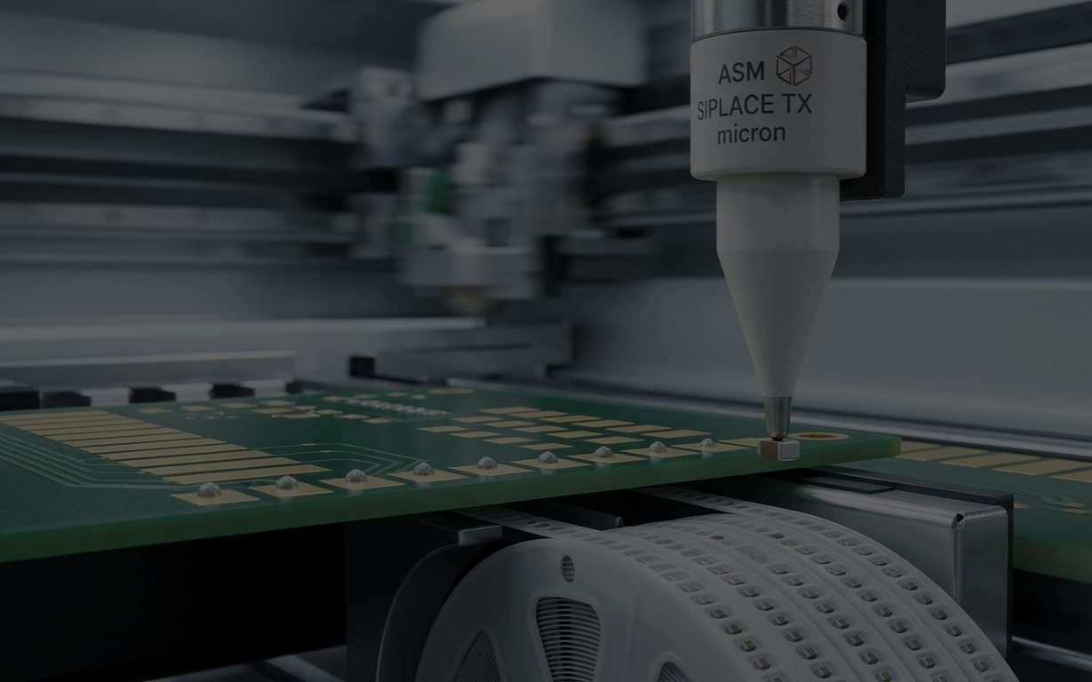
The real risk sits in downforce. 008004 and ultra-small multilayer ceramic capacitors have very low body compressive strength. If the Z axis does not decelerate and cushion at the instant of contact, the rigid impact fractures the micron-scale ceramic dielectric layers into micro-cracks that no naked eye or standard optical inspection will catch. These parts pass in-circuit test and only surface later as leakage, breakdown or opens once thermal cycling or vibration arrives. The countermeasure is a high-frequency voice coil motor with a closed-loop force sensor holding downforce at 0.5-1.0 N, with the velocity ramp completed before contact. Nozzle material and vacuum pressure belong to the same chain: a hard nozzle transmits impact straight into the body under high acceleration. Positional error feeds directly into tombstoning (the Manhattan effect). At small body sizes the surface-tension moment from the paste carries more relative weight, so a few microns of offset is enough to lift and rotate the part.
Mixed Lines: Bare Die, Flip Chip and SiP
SiP mounts logic, RF, memory and sensor dies alongside passives on one package substrate, so SMT equipment inherits work that used to belong to front-end packaging and the line between dispensing, placement and reflow blurs. The mixed line runs silicon, organic substrate, metal bumps and ceramic substrate at the same time, with a punishing CTE spread: silicon near 2.6 ppm/°C, organic substrate 15-20 ppm/°C, copper near 17 ppm/°C. During reflow cooling the layers contract out of step, shear piles up at the joints and in the intermetallic compound (IMC) layer, and Cu₆Sn₅ and Cu₃Sn keep growing thicker and more brittle through repeated thermal cycles until fatigue cracks nucleate; where copper and tin diffuse at different rates, Kirkendall voids are left behind at the interface. The industry response includes double-sided molding to cut package height, conformal EMI shielding that serves signal integrity and heat spreading at once, and laser-assisted bonding to sidestep the warpage and thermo-mechanical stress that conventional reflow bonding hits under CTE mismatch.
The SMT stage can only do so much: spread the stress, or lower the strain. Underfill and edge bonding spread it, taking shear strain that would otherwise sit at the joints across a larger interface and demoting the solder from primary load path to electrical interconnect; low-CTE, high-Tg epoxy systems lower it, cutting accumulated interfacial strain after cure. SCITEO low-shrinkage epoxy and edge-bonding materials for high-density assembly attack exactly those two quantities: cure shrinkage held below 0.06% gives micro-scale architectures a second load path running parallel to the metal joints.
Underfill and Edge Bond: The SMT Process View
Underfill is one of SCITEO's core product lines, and this section reads it strictly from the SMT process side: whether the fill runs a capillary-flow (CUF) or no-flow route, whether the cured material tolerates any further reflow passes, and whether its modulus and Tg can carry the load. Viscosity windows for small gaps, dispense paths and void-location judgment belong to the underfill discipline itself and are covered in a dedicated deep dive.
Edge bonding targets board-level thermal cycling. A continuous adhesive fillet runs around the package perimeter outside the joints, using lower modulus and higher elongation to absorb displacement between board and package. On modules that see multiple reflow passes, that fillet also limits how much a shield can or connector drags on joints under vibration. In automotive and industrial duty, that often counts for more than a strength number on its own.
Reflow Thermodynamics: Warpage, Head-in-Pillow and Void Control
Reflow is a coupled process: flux activation, oxide reduction, alloy melting and wetting, and IMC lattice growth all happen inside the same thermal window. SAC alloys melt at 217-219 °C, and full wetting usually needs a 235-250 °C peak with enough time above liquidus. Higher temperature and longer liquidus time raise the demands on materials and equipment together.
Dynamic Warpage, Head-in-Pillow and the Non-Wet Open Chain
Head-in-Pillow (HiP) is the hardest hidden defect to intercept on large, high-density BGA and multi-die packages. The chain starts with dynamic warpage: during ramp and soak, the die substrate and the PCB bow in opposite directions from uneven heating and CTE mismatch, lifting the corners and pulling BGA balls away from molten paste. Later in the reflow zone, stress releases as temperature stabilizes, the package flattens, and the balls settle back onto the pads. By then the flux activators are gone and both surfaces have oxidized. The two make physical contact without ever forming a metallurgical joint.
Such a joint passes in-circuit test and opens quickly under vibration or thermal cycling: a process pass that becomes a field failure. It has a close relative that gets confused with it, the non-wet open (NWO): ball and paste never coalesce at all, and a cross-section shows almost no solder on the pad. The two share a physical origin in dynamic warpage plus oxidation, but their acceptance windows and AXI slice signatures differ. Lumping them together sends corrective action in the wrong direction.
Controls have to press from several directions at once; single-point optimization does very little. Multi-zone forced convection compresses the lateral temperature difference ΔT so center and edge see comparable histories. A classic ramp-soak-spike, or a plateau profile on very high thermal mass assemblies, buys equalization time for large packages and multilayer high-frequency boards. Shadow Moiré or TherMoiré tracks the actual bow curve through ramp and holds board warpage within 0.05 mm/inch. Two variables get underestimated. Nitrogen reflow holding furnace oxygen below 1,000 ppm raises the warpage threshold at which Head-in-Pillow appears. Vacuum-assisted reflow during the liquidus stage takes dynamic warpage on high-mass substrates from the 0.15 mm range below 0.05 mm while suppressing oxidation and improving wetting. Multi-die packages and heavy-copper boards gain the most.
Void Rate and the Physical Window for Vacuum Reflow
A void is a cavity inside the joint. It reduces the effective cross-section for heat flow and current, and it acts as a stress concentrator where cracks nucleate. The documents are not interchangeable, so read the right one. IPC-A-610 gives general acceptability for void area fraction. BGA ball classification lives in IPC-7095, which sorts voids into Types A through E by location (inside the ball, at the package interface, at the PCB interface) with different limits for each; interface voids (Types D and E) are far more dangerous than voids inside the ball (Type C). QFN, SON and LGA bottom termination components (BTC) follow a different document again: IPC-7093 governs thermal-pad voiding. Automotive and medical programs tighten further on top, and balls on power or current paths get the lowest limits. That tightening is why vacuum reflow moved from an option to standard equipment.
Gas has two sources. Solvents and activators volatilize out of the flux, and moisture adsorbed by the PCB and components during storage and processing flashes to vapor at reflow. The second ties directly to moisture sensitivity level (MSL): bake and floor-life discipline per J-STD-020 and J-STD-033 removes a meaningful share of popcorn-related delamination and voids. The module's own bonding and sealing materials contribute as well. Adhesive already cured inside a cavity still releases a small amount of volatiles at a 235-250 °C peak, and molten solder captures it as voids. That is one reason SCITEO constrains total mass loss and volatile condensable materials together in its encapsulant formulations.
Vacuum reflow targets the escape path in the liquidus window. With the alloy molten and surface tension at its lowest, chamber pressure drops below 10 mbar, deep micro-bubbles expand under the pressure differential and rise out of the melt, and roughly 30 s of vacuum dwell at peak temperature takes large-pad void rates from the usual 10%-20% down below 2%. Pads with very large area, such as IGBT substrates, need more than vacuum: the expansion force of a bubble cannot overcome the capillary force of molten solder, so a 2-3 bar positive-pressure step after the vacuum squeezes the bubbles out. Fluxless routes use formic acid (HCOOH) to reduce metal oxide back to metal at 150-200 °C, leaving CO₂ and water to be purged with dry nitrogen, which removes both the cleaning step and the flux residue.
The craft is in timing and ramp rate. Pull vacuum too early and the molten solder is disturbed, spattering and shifting components; too late and the alloy has begun to solidify, locking bubbles into the solid phase. Heavy-copper AI server boards hold ball void rates below 1.8% by co-calibrating vacuum level with application timing.
High-Mass Boards and Multi-Pass Reflow: Material Endurance
High-density modules routinely need double-sided reflow, and complex RF or sensor assemblies reach a third pass. On the second pass the solder under a heavy component remelts, leaving mechanical support to adhesive that cured during the first pass. That is why printable SMT adhesive has stayed on mixed-technology lines. The stacked thermal load hits joints and module materials at once: joints show continued IMC growth and interface embrittlement, while cured adhesive shows modulus decay, outgassing and interfacial lift-off at temperature.
Multi-pass duty reduces to the question engineers ask most often: how many reflow passes can the material actually take. SCITEO high-temperature encapsulants handle three or more 260 °C peak reflow passes with no cracking, and hermeticity still holds after repeated passes. There is no padding in that number; it comes from running the real multi-pass profile, not a single oven soak. J-STD-020 moisture-sensitivity preconditioning itself requires devices to survive three consecutive reflow cycles, and high-reliability programs stack more passes on top. At the 200-300 °C class of long-term service, shear strength retention and insulation behavior go into the same formulation work, for power and sensor modules alike.
Selection needs four pieces of verifiable evidence. The short-term ceiling has to be more than a nameplate number: no damage through a 260 °C peak sustained across multiple reflow passes, while long-term endurance is reported as shear strength retention at the target duty cycle. Outgassing runs against ASTM E595, total mass loss (TML) and collected volatile condensable materials (CVCM), because volatiles in vacuum or sealed cavities contaminate optical surfaces and detectors. The last is ionic purity: mobile Na⁺ and Cl⁻ held to the 10 ppm range, which sets insulation life in humid environments.
Full-Chain 3D Inspection and the AI Closed Loop
At 008004 and sub-0.3 mm pitch, 2D vision has run out of discrimination. A 2D image carries no Z data, cannot resolve small differences in paste volume, cannot see the coplanarity problem created by a slightly lifted lead, and cannot look through a package body at the joints underneath. The workable path is to chain SPI, AOI and AXI into one measurement line and let the data drive process parameters back.
3D SPI: The Printer's Closed-Loop Data Source
3D SPI sits after the printer and before the placer. Rejecting boards is a byproduct; the real value is high-frequency feedback for the printing process. High-end systems use phase-modulated profilometry: a sinusoidal structured-light grating is projected onto the board, the grating picks up a phase shift where it lands on a paste deposit with height, and high-frequency camera arrays capture that shift so phase-shift algorithms can solve absolute volume, area, height and 3D shape for every deposit. On the line, each pad yields five core measurements: volume, height, area, XY offset and shape anomaly.
The statistics outweigh any single-board verdict. The printer is responsible for more than 70% of soldering defects, and intercepting them before reflow cuts final defect rates by 60%-80%. When volume data drifts in process-capability (Cpk) terms, a time series walks back to squeegee wear, gradual aperture clogging or print pressure drift. Rework becomes correction.
3D AOI: Post-Reflow Spatial Judgment
3D AOI sits after the reflow oven and makes the spatial call on final joint quality. Beyond phase-shift profilometry, high-end platforms add multi-angle projectors and high-tilt side camera arrays that break through part-body occlusion and reconstruct true 3D profiles of J-lead and gull-wing backsides. It is what checks 008004 parts for tombstoning, offset or flip, what judges wetting from fillet height and wetting angle on small joints, and what catches micron-scale coplanarity anomalies under a package.
Algorithm progress has concentrated on false calls. Rule-based judgment throws off a heavy false-call load on micro-components and low-contrast joints, while deep-learning defect classifiers trained on real line data cut false calls by more than a third and shorten the decision cycle. 3D-capable AOI now accounts for the majority of new installations, and its measurement data feeds process control platforms directly, cross-checking SPI paste-volume data.
3D AXI: Tomography Through the Package Body
For BGA, CSP, LGA and SiP, every joint sits directly under the package body. Visible light does not reach it, and 3D AOI with side optical paths does not either. 2D X-ray produces one grayscale overlay of the whole board, stacking top and bottom structures on each other and making Head-in-Pillow class discontinuities impossible to resolve. 3D AXI applies computed tomography: a microfocus X-ray tube and flat-panel detector sweep high-speed tilted trajectories, capturing hundreds of 2D projections of the region of interest, and a GPU runs algebraic reconstruction to generate high-resolution slices at different depths. Current systems reach ±50° tomography angles and 2 μm-class resolution on high-resolution configurations. This class of equipment moved onto volume production lines within the last two years and now brings Flip Chip and SiP micro-defects onto the same platform.
The capability that follows is direct. Process engineers can peel the BGA interior slice by slice, measure ball volume and deformation, locate voids in three dimensions, and identify regions where ball and pad touched without coalescing. Combined with deep-learning defect classification, decision stability stops depending on individual engineer experience, and every board's measurements accumulate as traceable data.
Data Loop and Yield Engineering
Inspection hardware pays off only when the data gets used. Feeding SPI, AOI and AXI output into the MES and SPC platform creates three loops: print parameters corrected from SPI volume trends, placement parameters compensated from AOI offset distributions, and reflow profiles adjusted locally from AXI void and non-wetting distributions. Two reverse indicators need watching at the same time. Push the false-call rate too high and the line will dial sensitivity down on its own; let the escape rate climb and real defects walk through. Both belong in the same scorecard. Root-cause traceability depends on time alignment: the loop only becomes engineering-grade when measurement timestamps, machine parameters and material lots resolve to the same board. SCITEO keeps the same lot-level records for its encapsulants, so the loop stays closed across a material change.
System Protection and Interface-Material Fit
Passing 3D AXI tomography means every internal electrical interconnect has met its acceptance limits. That only closes the internal logic. In humid outdoor radios, salt-spray industrial sites or vibration-heavy vehicle environments, exposed micro-circuitry can still fail through electrochemical migration (ECM) and leakage driven by trace moisture and ionic contamination, and in the worst case grows conductive anodic filaments (CAF). Protection has three layers: a continuous conformal coating at board level, local potting over sensitive devices and high-voltage pins, and encapsulation of larger cavities. The matching material numbers are shear retention after 85/85 damp-heat aging, volume resistivity, low outgassing and mobile ion content. SCITEO damp-heat-resistant epoxy sealing systems are built for exactly these duty cycles, bonding, sealing and filling critical BGAs, sensors and high-voltage pins so interconnect reliability extends across the service life of the system.
Process Window Quick Reference
The table below compresses the mechanisms above into numbers that can be checked directly in a design or process review:
| Process Stage | Typical Failure | Governing Criteria | SCITEO Direction |
|---|---|---|---|
| Stencil printing | Insufficient paste, skip print, bridging, solder beads | Area ratio ≥0.66 (≥0.75 on micro-components), transfer efficiency ≥95%, paste volume ±15% | Encapsulant systems with wide shear-rate windows and low ionic content |
| Micro-component placement | MLCC micro-cracks, tombstoning, offset | Downforce 0.5-1.0 N, placement accuracy ±15 μm, coplanarity | Low-modulus, low-shrinkage edge-bond materials |
| SiP heterogeneous integration | IMC fatigue, Kirkendall voids, delamination | CTE matching, Tg ≥150 °C, ions ≤10 ppm | Low-CTE underfill and edge-bonding materials |
| Reflow | Head-in-Pillow, non-wet open, dynamic warpage | Lateral ΔT control, warpage ≤0.05 mm/inch, ≥3 reflow passes | Reflow-resistant high-temperature bonding and thermal materials |
| Vacuum reflow | Voids, rising thermal resistance, reduced current path | Void rate <2%, pressure ≤10 mbar, 30 s vacuum dwell | Thermally conductive bonding and potting materials |
| Inspection and protection | Electrochemical migration, leakage, salt-spray corrosion | 3D AXI slice judgment, insulation resistance, hermeticity, ASTM E595 outgassing | Anti-aging epoxy and conformal coating materials |
Conclusion
On an 008004 land, the alloy in a single joint is measured in micrograms. Yet the process has to hold yield inside a controlled band across millisecond-scale shear, a contact force of a fraction of a newton, and a lateral temperature difference of a few degrees. Each quantity is measurable and each is coupled to the others, and when one crosses its limit the yield distribution records it.
Precision is rarely decided by a single machine or a single formulation. It is closer to an allocation: surface free energy between paste and aperture wall, contact force between component and pad, expansion difference between adhesive and substrate, heat flow between package and system. Every interface redistributes stress, heat and time. SCITEO works at those interfaces, turning the allocation into boundaries that can be calculated and verified.
This article is SCITEO Advanced Materials original technical content; unauthorized reproduction is prohibited.
Appendix: Process & Engineering Adhesive FAQ Index
In an 008004 process, how do you break the stencil area-ratio bottleneck that causes skip print?
Geometry first. Area ratio is aperture bottom area divided by aperture wall area, and the IPC-7525 floor is 0.66; 008004 apertures should target 0.75, with local step thinning to cut the wall share. Then the interface: laser cutting, electropolishing, electroforming, and a monolayer anti-stick nano-coating that drops aperture-wall surface free energy so paste-to-wall adhesion falls below paste-to-pad adhesion. Then rheology: squeegee speed and pressure have to track the paste shear-thinning curve and thixotropic recovery time, liquefying fully during fill and recovering yield stress in milliseconds during separation. With all three in place, transfer efficiency on sub-micron apertures holds above 95% and paste volume converges inside ±15%. Powder size is the fourth lever people forget: 008004 generally needs Type 6 (5-15 μm) or even Type 7 (2-11 μm) powder, so five or six of the largest particles still span the aperture and keep flow continuous.
What is the thermodynamic root cause of Head-in-Pillow in high-density BGA reflow?
Dynamic warpage, not peak temperature. During ramp and soak, the die substrate and the PCB bow in opposite directions from CTE mismatch and uneven heating, lifting the package corners and pulling the BGA balls out of molten paste. Later in the reflow zone, stress release flattens the package and the balls touch down again, but the flux activators are already gone and both surfaces are oxidized, so the interface makes physical contact without metallurgical bonding. In-circuit test passes and the joint opens under the first mechanical or thermal load. Keep it distinct from the non-wet open (NWO), where ball and paste never coalesce at all and a cross-section shows almost no solder on the pad; the corrective action differs. Controls run in three layers: compress the lateral temperature difference ΔT with multi-zone forced convection, use a long soak or plateau profile so high-mass packages and heavy-copper boards reach thermal equilibrium, and track the actual bow curve with shadow Moiré or TherMoiré to hold board warpage inside 0.05 mm/inch. Nitrogen reflow below 1,000 ppm oxygen also raises the warpage threshold at which HiP appears, and it pays for itself.
How do you hold void rates below 2% on large thermal pads under IGBT or QFN packages?
Vacuum reflow is the enabling process. Under atmospheric reflow, flux volatiles and PCB outgassing are trapped inside liquid solder and large-pad void rates stall between 10% and 20%, while voids both concentrate stress and cut the effective cross-section for heat and current. Vacuum reflow pulls the chamber below 10 mbar during the liquidus window, when surface tension is at its lowest, so deep micro-bubbles expand under the pressure differential and rise out of the melt, with roughly 30 s of vacuum dwell at peak temperature. On very large pads such as IGBT substrates, vacuum alone is not enough: bubble expansion cannot beat the capillary force of molten solder, so a 2-3 bar positive-pressure step after the vacuum squeezes the gas out. The hard part is the timing and ramp rate, not the vacuum level; too early disturbs the melt and causes spatter and component shift, too late and the alloy has begun to solidify and locks bubbles in the solid phase. With vacuum level and timing co-calibrated, heavy-copper AI server substrates hold ball void rates below 1.8%. Check the limits in the right document: IPC-7095 for BGA balls, IPC-7093 for the thermal pad on QFN and LGA bottom termination components. The two are not interchangeable.
Why does capillary underfill under a BGA or SiP keep producing voids or delamination?
Voids usually come from the process side, not from the material. Substrate preheat is too low, so viscosity stays high and capillary driving force is weak, and the flow front entraps gas. The dispense path is poorly planned, so converging fronts seal the vent early; an L or U pattern advancing from one side gives gas an escape route. Flux residue on pads and solder mask is left in place and changes local surface tension until wetting fails. Delamination tracks thermo-mechanical values that have to be read in pairs: glass transition temperature sets the modulus platform at service temperature and CTE sets accumulated interfacial shear strain. SCITEO designs Tg and CTE as one pair in these underfill systems, constraining cure shrinkage and mobile ion content alongside them, because residual stress built in during cure and ion migration under damp heat usually decide failure earlier than initial strength does. One thing is easy to miss: a void at the joint root is far more dangerous than a void at the edge, so judgment has to combine void area fraction with location.
What actually separates 3D AXI from 2D X-ray, and what does AI add?
2D X-ray collapses the whole board into one grayscale overlay, stacking top and bottom joints on each other, so it cannot resolve a discontinuity class such as Head-in-Pillow. 3D AXI applies computed tomography: a microfocus X-ray tube and flat-panel detector sweep high-speed tilted trajectories to capture hundreds of projections from different angles, and a GPU runs algebraic reconstruction (ART) to produce high-resolution slices at depth, with tomography angles up to ±50° and 2 μm-class resolution on high-resolution configurations. Engineers can then measure ball volume, deformation and three-dimensional void coordinates slice by slice. AI adds the classification layer: deep-learning defect models cut false calls from rule-based algorithms by about a third and turn every board's verdict into traceable data for closed-loop correction of print and placement parameters.
When a board sees two or three reflow passes, which material metrics should be qualified?
Start with the number everyone asks for first: how many passes. SCITEO high-temperature encapsulants take three or more 260 °C peak reflow passes with no cracking, and hermeticity still holds after repeated passes; J-STD-020 moisture-sensitivity preconditioning already uses three reflow cycles as the pass condition, and high-reliability programs stack more passes on top of that. Beyond the count, four pieces of evidence decide the material: long-term endurance reported as shear strength retention at the 200-300 °C class for the target duty cycle rather than a nameplate temperature; outgassing measured as total mass loss and collected volatile condensable materials per ASTM E595, because volatiles in vacuum or sealed cavities contaminate optical surfaces and detectors; ionic purity holding mobile Na⁺ and Cl⁻ to the 10 ppm range; and structural strength judged from interface lift-off after repeated passes, not from an initial value alone. Only when all four hold does the material keep insulation, thermal conduction and hermeticity stable across double-sided reflow and subsequent aging.